
Author
Author

Barry Olney is the Executive Director of In-Circuit Design Pty Ltd (iCD) in Australia. The company specializes in PCB design services and focuses on circuit board-level simulation technology.
The iCD Design Integrity software developed by the company integrates iCD Stackup, PDN, and CPW Planner. This software can be downloaded from www.icd.com.au.
The layout of components on a PCB is more complex than simply fitting parts into available space. It plays a critical role in determining the overall manufacturability, performance, reliability, and cost of the PCB. Poor layout can even affect the most carefully designed PCBs.
An effective component layout can alleviate mechanical stress, promote efficient thermal management, and help prevent excessive heat buildup. Conversely, a poor layout can lead to soldering obstacles, assembly and testing challenges, increased layer counts, signal integrity issues, power noise, and electromagnetic compatibility failures.
Anyone who thinks component layout is easy has never dealt with RF or high-speed layouts.This article will delve into the factors that need to be considered for high-speed PCB layouts, making effective board planning both an art and a science.

Figure 1: Grouping components logically and functionally
It is recommended to group components based on rise time and operating frequency, positioning the fastest devices closest to the connectors, as shown in Figure 1.
Subsequent placements should follow the descending order of signal speed, with analog sections located farthest from the connectors to reduce the risk of noise coupling into sensitive circuits.
Electrical isolation should be maintained for switching mode power supplies while keeping a continuous common ground plane. Special attention should be paid to minimizing net crossings to improve routing efficiency.
All analog signals should be routed within the analog area, while digital signals should be confined to the digital area, both sharing a continuous common ground plane, which is crucial.
Control signals can be passed between these areas as needed. Over the years, I have implemented an effective method for achieving this isolation: routing isolation fences or no-route zones.
We achieve isolation by placing narrow no-route zones between signal layers, effectively guiding the routing process and preventing signals from crossing designated boundaries on specific layers. Figure 1 illustrates a typical application of this technique.
Remember, high-speed return currents follow the path of least inductance. For example, when a trace extends from an Analog-to-Digital Converter (ADC) to an FPGA, the return current will flow directly beneath that trace, avoiding nearby areas.
Routing isolation fences can also help control the automatic router by preventing signals from crossing boundaries while allowing control signals to pass through.
Since crosstalk is caused by interference signals coupling onto victim signals, higher interference signal voltages will cause more crosstalk. To mitigate this, it is recommended to isolate net groups based on signal amplitude. This can prevent higher voltage nets (like 3.3V) from affecting lower voltage nets (like 1.5V) with reduced noise margins.
Signal transmission time and skew are critical factors to consider in high-speed PCB design. The primary factors affecting these parameters are the layout of components.
By controlling the layout of devices and assuming adherence to good design practices, the maximum signal delay can be approximated as the longest Manhattan (X+Y) distance within a specific clock domain.
First, route clock/through signals within a group without initially using serpentine patterns. This allows for precise skew matching later in the process, as nets with higher signal speeds can be lengthened to align with the longest propagation delay, ensuring that signals arrive synchronously across all critical paths.
Clocks should always have the longest delay, allowing data and address lines time to stabilize before being sampled. Therefore, the transmission time and skew across the entire clock domain are determined by the maximum placement and routing rules that enforce trace delay matching.
However, there is a critical point. If the distance between the controller and memory is too close, trace adjustments become challenging; if too far, signal propagation delays increase.
In traditional high-speed design workflows, timing specifications and simulation results should serve as the basis for establishing layout and routing constraints. Given the delay constraints, designers can manage signal integrity by controlling the PCB routing topology of different interface components.
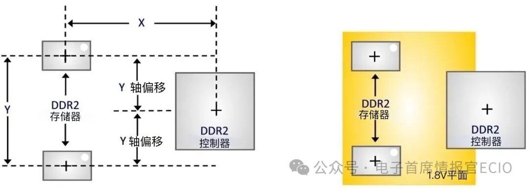
Figure 2: Layout requirements for processor and memory devices on a 1.8V plane
Figure 2 shows the layout requirements for DDR2 controllers and memory chips, as well as the 1.8V power plane.
However, it applies to all memory interfaces. The layout guidelines aim to limit maximum trace delays and address routing and via layout challenges. Notably, this layout approach does not specify whether these devices are laid out on the top or bottom of the circuit board.
DDR circuit areas must be isolated from other signals to prevent interference while maintaining a common ground plane.
As shown in Figure 2, the specified no-route zones can achieve this goal. The 1.8V power plane should cover the entire area, and non-DDR signals should remain outside of it to maintain signal integrity and proper operation.
Additionally, layout challenges may arise when placing series termination devices. When there is no termination at the far end of the trace, series terminations must be positioned to effectively absorb the full reflection of the load return.
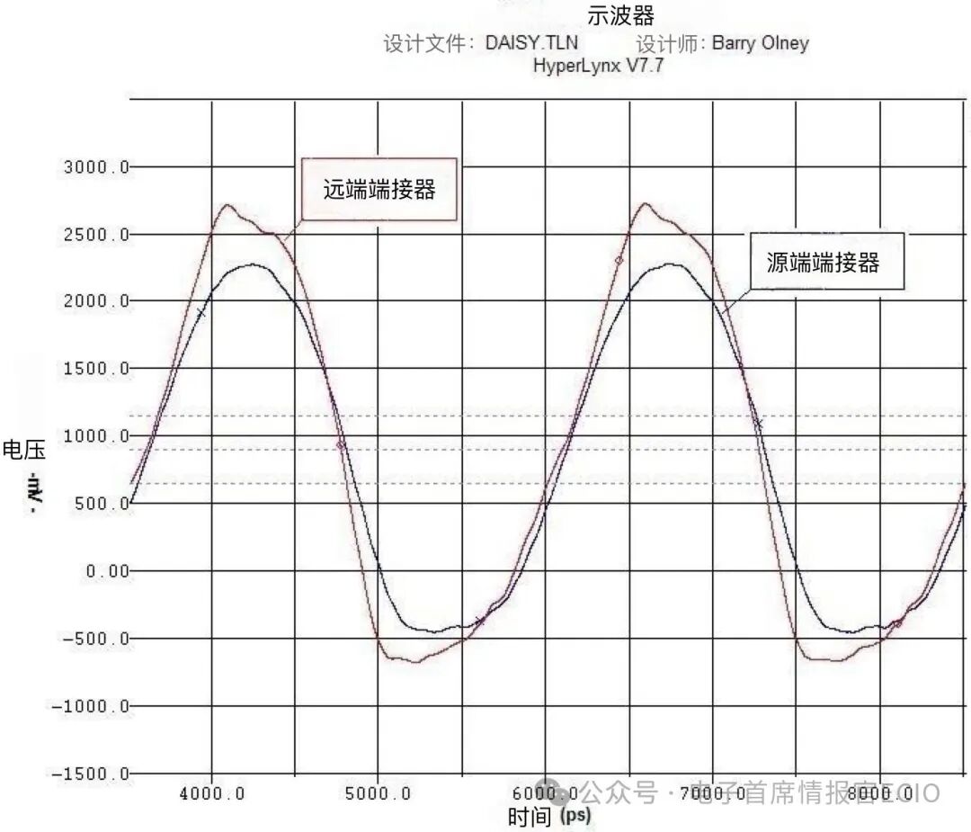
Figure 3: Differences between series terminations at the source and load ends.
Figure 3 illustrates the difference between placing series terminations near the source (which is common) and placing them at the far end near the load (which is generally not recommended). Both positions are used to absorb reflections before they propagate multiple times along the trace.
However, far-end terminations often produce more waveform distortion, while near-end terminations yield clearer signals. Additionally, parallel terminations may be needed to address VTT pull-up issues.
These are typically laid out at the end of a daisy chain, pulling the signal to the DDR2 reference voltage VTT. Proper layout at the end of traces is crucial.
Effective component layout is essential for maintaining high-speed signal integrity, efficient power distribution, thermal management, and manufacturability. Coordinating this with stackup planning, which determines routing paths, impedance levels, and return current behavior, is vital.
Some tools provide precise dielectric control to facilitate optimal layouts for critical components such as clocks, SerDes, and DDR memory, thereby reducing stub lengths, skew, and via counts.
Isolating nets based on voltage, rise time, and function—using routing fences and no-route zones—helps mitigate crosstalk and EMI.
Furthermore, controlling component spacing to manage transmission times ensures timing consistency across clock domains. Proper layout of terminations and power decoupling components, especially within DDR interfaces, can further enhance signal quality and overall system reliability.
Key Points
-
First, establish the stackup structure. Use the stackup to determine which layers sensitive nets should be located on, then layout components to ensure no switching signals between these stackups.
-
Group components based on rise time and operating frequency, placing the highest-speed devices closest to the connectors.
-
All analog signals should be routed within the analog area, while digital signals should be confined to the digital area, both sharing a continuous common ground plane.
-
Set no-route zones on signal layers to effectively guide the routing process and prevent signals from crossing designated boundaries on specific layers.
-
Group nets based on signal amplitude for isolation.
-
In high-speed PCB design, signal transmission delay and skew are critical factors to consider.
-
By properly controlling the layout of devices, the maximum signal delay can be approximated by the longest Manhattan distance (X + Y) within a specific clock domain.
-
Clock signals should always have the longest delay to allow data and address lines sufficient time to stabilize before being sampled.
-
Timing specifications and simulation results should serve as the basis for establishing component layout and routing constraints.
-
DDR circuit areas must be isolated from other signals to prevent interference while maintaining a common ground plane.
-
It is recommended to layout termination devices within 200 mils (approximately 5 mm) of the signal source.
References
Beyond Design by Barry Olney: “Critical Placement,” “The Fundamental Rules of High-Speed PCB Design Part 2,” “Interactive Placement and Routing Strategies.”


These are electronic chief information officer partners(partial)
Order does not imply priority