
Due to the distributed parameter nature of radio frequency (RF) circuits, skin effect and coupling effects can easily occur during actual circuit operation, making it difficult to control interference radiation in PCB design.
For example, issues such as interference between digital and analog circuits, noise interference from power supplies, and interference caused by unreasonable grounding can arise.
Therefore, how to weigh the pros and cons during the PCB design process to find a suitable compromise, minimizing these interferences and even avoiding some circuit interference, is key to the success of RF circuit PCB design.
This article provides some techniques from the perspective of PCB layout that are useful for improving the anti-interference capability of RF circuits.
 1RF Layout
This section mainly discusses the component placement layout of multilayer boards.
The key to component placement layout is to fix the components located on the RF path, adjusting their orientation to minimize the length of the RF path, and to keep the input as far away from the output as possible, separating high-power circuits from low-power circuits, and sensitive analog signals from high-speed digital signals and RF signals.
Some common techniques used in layout include:
1Linear Layout
Components for the main RF signal should be arranged in a linear layout as much as possible, as shown in Figure 1.
However, due to the limitations of PCB and cavity space, it is often not possible to arrange them in a straight line. In such cases, an L-shape can be used, and a U-shape layout should be avoided (as shown in Figure 2). If unavoidable, try to increase the distance between the input and output to at least 1.5 cm.
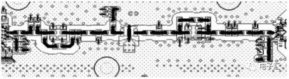
Figure 1 Linear Layout
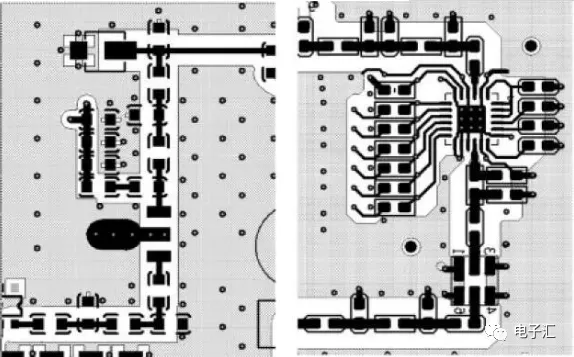
Figure 2 L-shaped and U-shaped Layouts
Additionally, when using L-shaped or U-shaped layouts, the turning point should not turn immediately upon entering the interface, as shown in the left of Figure 3, but should turn after a short straight section, as shown in the right of Figure 3.
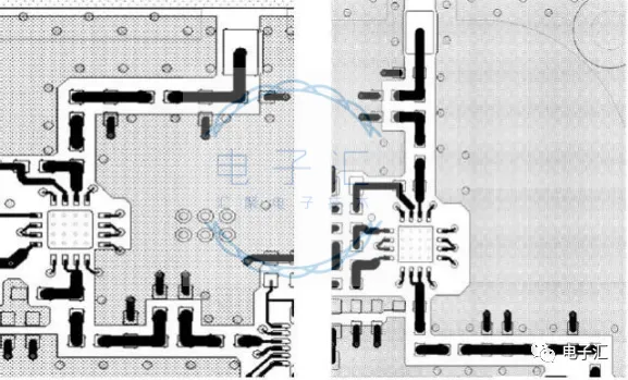
Figure 3 Two Schemes
2Identical or Symmetrical Layout
Identical modules should be arranged in the same or symmetrical layout as much as possible, as shown in Figures 4 and 5.
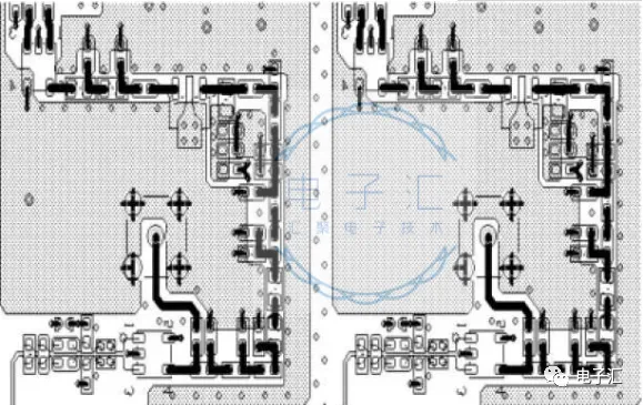
Figure 4 Identical Layout
Figure 5 Symmetrical Layout
3Cross Layout
The feed inductance of the bias circuit should be placed perpendicular to the RF channel, as shown in Figure 6, mainly to avoid mutual inductance between inductive components.
Figure 6 Cross Layout
445-Degree Layout
To make reasonable use of space, components can be arranged at a 45-degree angle to keep RF lines as short as possible, as shown in Figure 7.
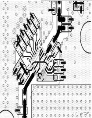
Figure 7 45-Degree Layout
 2RF Wiring
The overall requirement for wiring is: RF signal traces should be short and straight, minimizing abrupt changes, avoiding vias, and not intersecting with other signal lines. Additionally, as many ground vias as possible should be added around the RF signal line.
Here are some commonly used optimization methods:
1Gradient Line Processing
When the width of the RF line is significantly larger than the width of the IC device pins, the width of the line contacting the chip should adopt a gradient approach, as shown in Figure 8.
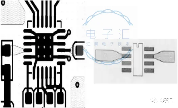
Figure 8 Gradient Line
2Arc Line Processing
If the RF line cannot be straight, it should be processed into an arc line, which can reduce RF signal radiation and mutual coupling. Experiments have shown that using curved right angles for transmission line corners can minimize return loss, as shown in Figure 9.
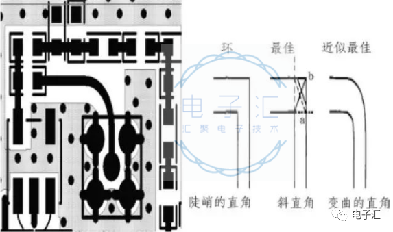
Figure 9 Arc Line
3Ground and Power Supply
Ground lines should be as thick as possible. If conditions allow, every layer of the PCB should be covered with ground, and the ground should be connected to the main ground, with as many ground vias as possible to reduce ground line impedance.
RF circuit power supplies should avoid using planar segmentation; a solid power plane not only increases radiation from the power plane to RF signals but is also easily interfered with by RF signals. Therefore, power lines or planes should generally be in a long strip shape, processed according to the current size, being as thick as possible while meeting current capacity, but not excessively wide. When processing power lines, it is essential to avoid forming loops.
The direction of power lines and ground lines should be parallel to the direction of RF signals but should not overlap. Where they cross, it is best to use a vertical cross.
4Cross Processing
RF signal lines should cross IF signal lines, with as much ground as possible in between.
When RF signal lines cross with other signal lines, a layer of ground connected to the main ground should be arranged along the RF signal line between them. If this is not possible, they must be guaranteed to cross at right angles. Other signal lines also include power lines.
5Ground Enclosure Processing
Ground processing for RF signals, interference sources, sensitive signals, and other important signals can improve the anti-interference capability of these signals and reduce their interference with other signals, as shown in Figure 10.
Figure 10 Ground Enclosure Processing
6Copper Foil Processing
Copper foil processing requires smooth and flat surfaces, with no long lines or sharp corners. If unavoidable, add several ground vias at sharp corners, thin copper foils, or the edges of copper foils.
7Spacing Processing
RF lines should be at least 3W away from the edges of adjacent ground planes, and there should be no non-ground vias within the 3W range.
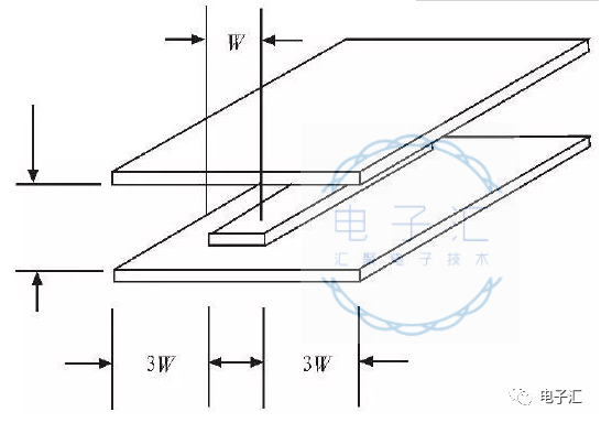
Figure 11 Spacing
RF lines on the same layer should be enclosed with ground, and ground vias should be added to the ground copper skin. The spacing between vias should be less than 1/20 of the wavelength (λ) corresponding to the signal frequency, arranged uniformly and neatly. The edge of the ground copper skin should be 2W away from the RF line or 3H away, where H represents the total thickness of the adjacent dielectric layers.
 3Cavity Processing
For the entire RF circuit, RF units of different modules should be isolated using cavities, especially between sensitive circuits and strong radiation sources. In high-power multi-stage amplifiers, isolation between stages should also be ensured.
Once the entire circuit branch is properly placed, the processing of the shielding cavity should be addressed. The following are important considerations for processing the shielding cavity:
The entire shielding cavity should be made into a regular shape for easy molding. Each shielding cavity should be rectangular, avoiding square shielding cavities.
The corners of the shielding cavity should be rounded, and the shielding metal cavity is generally molded. Rounded corners facilitate mold release during casting, as shown in Figure 12.
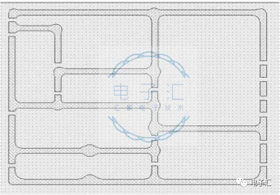
Figure 12 Cavity
The perimeter of the shielding cavity should be sealed, and the leads into the cavity should generally use strip lines or microstrip lines, while different modules inside the cavity should use microstrip lines. The connections between different cavities should be slotted, with a slot width of 3mm, and the microstrip line should run in the center.
3mm metallized holes should be placed at the corners of the cavity to secure the shielding shell, and equal metallized holes should be evenly placed on each long cavity for reinforcement.
The cavity should generally have window openings for easy welding of the shielding shell, with a thickness of more than 2 mm, and two rows of window vias should be added to the cavity, with the vias staggered and spaced 150 MIL apart within the same row.
 4Conclusion
The key to the success of RF circuit PCB design lies in how to reduce circuit radiation to improve anti-interference capability. However, in actual layout and wiring, some issues may conflict, so finding a compromise to optimize the overall performance of the RF circuit is a problem that designers must consider.
All of this requires designers to have a certain level of practical experience and engineering design capability. However, it is impossible for every designer to acquire these abilities overnight; only by learning from others’ experiences and continuously exploring and thinking can one make progress.
This article summarizes some design experiences from work, which are beneficial for improving the anti-interference capability of RF circuit PCBs and helping beginners in RF circuit design avoid unnecessary detours.

 Four Basic Characteristics of PCB RF Circuits
This article interprets the four basic characteristics of RF circuits from the aspects of RF interface, small expected signals, large interference signals, and adjacent channel interference, and provides important factors that need special attention during PCB design.
1RF Circuit Simulation of RF Interface
Wireless transmitters and receivers can conceptually be divided into baseband and RF components.
The baseband includes the frequency range of the input signal of the transmitter and the frequency range of the output signal of the receiver.
The bandwidth of the baseband determines the basic rate at which data can flow through the system.
The baseband is used to improve the reliability of data flow and reduce the load imposed by the transmitter on the transmission medium at specific data transmission rates.
Therefore, when designing baseband circuits on PCBs, a significant amount of signal processing engineering knowledge is required.
The RF circuit of the transmitter can convert the processed baseband signal and upconvert it to the designated channel, injecting this signal into the transmission medium.
Conversely, the RF circuit of the receiver can obtain signals from the transmission medium and convert and downconvert them to baseband.
The transmitter has two main PCB design goals:First, they must transmit a specific power while consuming as little power as possible.Second, they must not interfere with the normal operation of transceivers in adjacent channels.
For receivers, there are three main PCB design goals: first, they must accurately restore small signals; second, they must be able to eliminate interference signals outside the desired channel; and lastly, like transmitters, they must consume very little power.
2RF Circuit Simulation of Large Interference Signals
Receivers must be sensitive to small signals, even in the presence of large interference signals (obstacles).
This situation occurs when trying to receive a weak or distant transmission signal while a powerful transmitter is broadcasting in an adjacent channel.
Interference signals can be 60-70 dB larger than the expected signal and can cover the receiver’s input stage significantly or cause excessive noise at the input stage, blocking the reception of normal signals.
If the receiver’s input stage is driven into a nonlinear region by the interference source, the above two problems will occur. To avoid these issues, the front end of the receiver must be very linear.
Thus, “linearity” is also an important consideration in PCB design for receivers.
Since receivers are narrowband circuits, nonlinearity is statistically measured by “intermodulation distortion”.
This involves driving the input signal with two closely spaced sine or cosine waves located within the center band (in band) and then measuring their intermodulation products.
Generally, SPICE is a time-consuming and costly simulation software because it must perform many cycles of calculations to achieve the required frequency resolution to understand distortion conditions.
3RF Circuit Simulation of Small Expected Signals
Receivers must be highly sensitive to small input signals. Generally, the input power of receivers can be as low as 1 μV.
The sensitivity of the receiver is limited by the noise generated by its input circuit. Therefore, noise is an important consideration in PCB design for receivers.
Moreover, the ability to predict noise using simulation tools is essential. Figure 1 shows a typical superheterodyne receiver. The received signal first passes through filtering and is then amplified by a low-noise amplifier (LNA).
Then, the first local oscillator (LO) mixes with this signal to convert it to intermediate frequency (IF). The noise performance of the front-end circuit mainly depends on the LNA, mixer, and LO.
While traditional SPICE noise analysis can find the noise of the LNA, it is useless for the mixer and LO because the noise in these blocks is severely affected by the large LO signal.
Small input signals require the receiver to have a very high gain, typically needing as high as 120 dB. At such high gain, any signal that couples back from the output to the input can cause problems.
The importance of using a superheterodyne receiver architecture is that it can distribute gain across several frequencies to reduce the likelihood of coupling.
This also ensures that the frequency of the first LO is different from the frequency of the input signal, preventing large interference signals from “polluting” small input signals.
For various reasons, in some wireless communication systems, direct conversion or homodyne architectures can replace superheterodyne architectures.
In this architecture, the RF input signal is directly converted to baseband in a single step, so most of the gain is in the baseband, and the LO frequency is the same as the input signal frequency.
In this case, the impact of minimal coupling must be understood, and a detailed model of the “stray signal path” must be established, such as coupling through the substrate, coupling between package pins and bond wires, and coupling through power lines.
4RF Circuit Simulation of Adjacent Channel Interference
Distortion also plays an important role in transmitters. Nonlinearity generated in the output circuit of the transmitter can cause the transmitted signal’s bandwidth to spread into adjacent channels. This phenomenon is known as “spectral regrowth”.
Before the signal reaches the power amplifier (PA) of the transmitter, its bandwidth is limited; however, intermodulation distortion within the PA can cause the bandwidth to increase again. If the bandwidth increases too much, the transmitter will not meet the power requirements of its adjacent channels.
When transmitting digitally modulated signals, it is practically impossible to predict spectral regrowth using SPICE. This is because approximately 1000 digital symbols must be simulated to obtain a representative spectrum, and high-frequency carriers must also be combined, making SPICE’s transient analysis impractical.

Some Screenshots from Electronic Books

【Complete Set of Hardware Learning Materials Collection】