The standard design process that PCB (Printed Circuit Board) engineers must master is crucial for ensuring the performance, reliability, and manufacturability of circuit boards. Below is a phased outline of the standard design process and its core points:
1. Requirement Analysis and Preliminary Preparation
-
Clarify Design Objectives
-
Define circuit functions and performance indicators (such as signal rate, power supply voltage, power consumption, etc.).
-
Clarify the physical constraints of the PCB (size, number of layers, mounting methods, heat dissipation requirements, etc.).
-
Confirm special requirements (such as high frequency, high speed, high density, impedance control, EMC/EMI compatibility, etc.).
-
Collect Design Data
-
Schematic: Confirm component packaging, network connections, power/ground distribution.
-
Component Library: Verify the packaging dimensions, pin definitions, and 3D models of all components (to avoid library errors that could lead to production issues).
-
Mechanical Structure Diagram: Confirm the fit dimensions of the PCB with the enclosure, connectors, and heat sinks.
-
Manufacturing Specifications: Understand the process capabilities of PCB manufacturers (minimum line width/spacing, hole diameter, lamination structure, etc.).
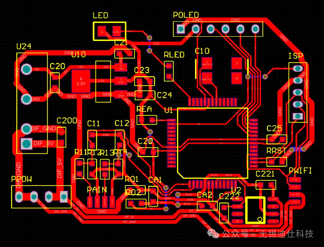
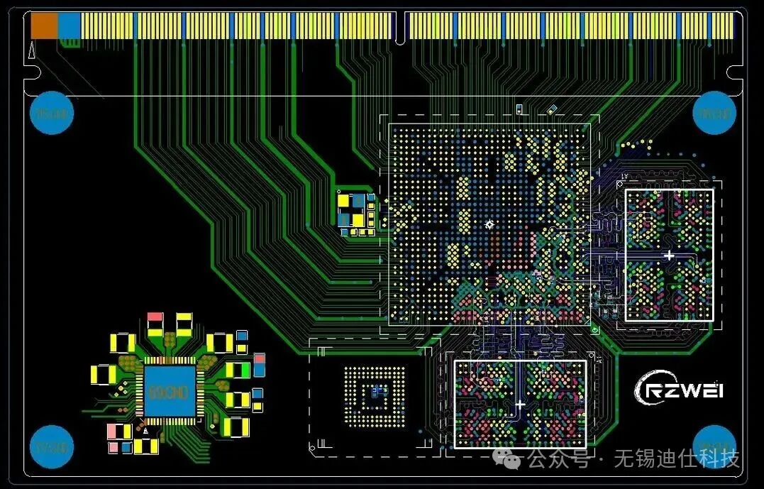
2. PCB Layout Design (Placement)
-
Layer Planning
-
Allocate layers based on signal types (e.g., high-speed signals on inner layers, power/ground on outer layers).
-
Determine the stacking structure (e.g., 4-layer board: Top signal layer, GND layer, Power layer, Bottom signal layer).
-
Label impedance control requirements (e.g., differential pairs, single-ended line impedance values).
-
Modular Layout
-
Divide areas by function (e.g., power module, digital circuit, analog circuit, RF circuit).
-
Prioritize the layout of key components (e.g., CPU, FPGA, high-frequency devices, connectors).
-
Follow the principle of “large first, small later; difficult first, easy later” to reduce layout adjustment times.
-
Thermal Design
-
Distribute high-power components (e.g., MOSFETs, LDOs) evenly to avoid localized overheating.
-
Reserve thermal pads or holes, and add heat sinks or thermal materials if necessary.
-
Keep analog circuits away from digital noise sources (e.g., switch power supplies, clock circuits).
3. PCB Routing Design
-
Signal Integrity (SI) Design
-
High-Speed Signals: Use differential pairs, impedance matching, avoid right-angle bends, and control line length matching.
-
Sensitive Signals: Isolate analog signals from digital signals, and shield or ground critical signals (e.g., clock, reset).
-
Power Integrity (PI): Reasonably divide power planes, design wide traces for high current paths, and place decoupling capacitors close to power pins.
-
EMC/EMI Design
-
Reduce loop area (e.g., power/ground return loops).
-
Add filter capacitors or ferrite beads to critical signals.
-
Avoid long parallel traces to reduce crosstalk.
-
Design for Manufacturability (DFM)
-
Follow the PCB manufacturer’s specifications for minimum line width/spacing, hole diameter, and pad sizes.
-
Avoid isolated copper and sharp angles (which can cause acid etching residues).
-
Ensure clear silkscreen markings (component polarity, test points, version numbers).
-
Design panelization (V-Cut or postage hole) to improve production efficiency.
4. Design Verification and Inspection
-
Design Rule Check (DRC)
-
Use EDA tools (such as Altium Designer, Eagle, KiCad) to run DRC, checking for shorts, opens, spacing violations, etc.
-
Manually check the continuity of critical networks (e.g., power, ground, high-speed signals).
-
Signal Integrity Simulation (SI Simulation)
-
Simulate impedance, crosstalk, and timing for high-speed signals (e.g., USB, HDMI, DDR).
-
Optimize termination resistors, line length matching, and other parameters.
-
Thermal Simulation and Mechanical Verification
-
Use thermal simulation tools (such as FloTHERM) to verify thermal design.
-
Check for interference between the 3D model and mechanical structures (e.g., connector, heat sink installation space).
5. Output Files and Production Preparation
-
Gerber File Generation
-
Export Gerber files for each layer (Top/Bottom copper layers, silkscreen layer, solder mask layer, drill layer, etc.).
-
Generate drill files (NC Drill File) and assembly drawings (Assembly Drawing).
-
BOM and Placement Files
-
Generate an accurate Bill of Materials (BOM), including component models, packaging, quantities, and supplier information.
-
Provide placement coordinate files (Pick & Place File) for SMT production.
-
Communicate with PCB Manufacturers
-
Confirm process capabilities (e.g., surface treatment processes: gold plating, tin spraying, OSP).
-
Attach special requirement notes (e.g., impedance control, blind/buried vias, back drilling) when submitting design files.
6. Design Optimization and Iteration
-
Prototype Testing and Debugging
-
Conduct functional testing and signal quality testing (such as eye diagrams, timing analysis) after producing PCB prototypes.
-
Document issues (such as noise, overheating, signal attenuation), analyze causes, and optimize the design.
-
Design Review
-
Summarize lessons learned from the design (such as unreasonable layout, routing violations).
-
Update design specifications and component libraries to avoid repeating mistakes.
Key Standards and References
-
IPC Standards: IPC-2221 (General Design Guidelines), IPC-6012 (Rigid Board Performance Specifications).
-
Signal Integrity: IEEE 802.3 (Ethernet), USB 2.0/3.0/4.0 specifications.
-
EMC Design: CISPR 32 (Electromagnetic Compatibility Standards), FCC Part 15 (U.S. Radio Interference Regulations).
By following the standard design process, PCB engineers can significantly improve design efficiency, reduce manufacturing costs, and ensure that products meet performance and reliability requirements.