In working circuit boards, there are many components that generate significant heat, such as MOSFETs, LEDs, and transistors, especially under full load conditions. Heat dissipation vias are a well-known method for dissipating heat through surface-mounted components on circuit boards. Structurally, a via is drilled into the board, and if the board is a single-layer or double-sided board, copper foil connects the top and bottom surfaces of the PCB to increase the area and volume available for heat dissipation, thereby reducing thermal resistance. In the case of multilayer boards, thermal vias can connect multiple layers, or may be limited to partial connections between layers, but in all cases, the basic principle remains the same.
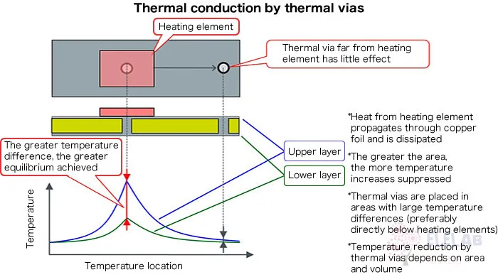
Mounting the heat sink pads of surface-mounted components on the PCB can reduce thermal resistance. Thermal resistance depends on the area and thickness of the copper foil used for heat dissipation on the PCB, as well as the thickness and material of the board. Essentially, the wider and thicker these materials are, the greater the heat dissipation effect. However, the thickness of the copper foil usually needs to meet standard specifications and cannot be excessively thick. Additionally, since miniaturization remains a fundamental design requirement, the area of the PCB should be designed according to actual needs, and the actual thickness of the copper foil cannot be made excessively large. Thus, when the PCB exceeds a certain single-sided heat dissipation area, the heat dissipation effect of a single-sided circuit board will be greatly compromised. The thermal conductivity of FR-4 is very low.One measure to solve these problems is to use thermal vias, which are formed by drilling and plating copper, similar to PTH or vias used for electrical interconnection between layers. For effective use of heat dissipation vias, they should be placed close to the heating components. As shown in the figure below, utilizing the effect of thermal balance, it is evident that connecting areas with large temperature differences will yield good results.
Impact of Hollow Vias vs. Filled Vias
Hollow vias, compared to filled vias, will lead to higher thermal resistance. For a via with a diameter of 0.6mm, using 35 um (1 oz.) plated copper, the area perpendicular to the thermal pad is only 0.06 mm², while the area of a solder-filled via is 0.28 mm², resulting in a thermal resistance of 64°C/W, while the filled solder results in 42°C/W, and if completely filled with copper, it would be 14°C/W. Compared to vias filled with SnAgCu solder, the ability of solid (copper) filled vias can further reduce thermal resistance.
Increasing the plating thickness during the PCB manufacturing process will improve the thermal resistance of the vias. In the above example, increasing the plating thickness to 70 um (2 oz.) will reduce the thermal resistance of each via to 34°C/W. However, this will increase the cost of PCB production.
In addition to creating solid vias during the PCB production plating process, another option is to fill the vias with copper (or other thermally conductive materials, such as conductive epoxy) during PCB production. However, this adds an additional step in PCB manufacturing, potentially increasing the cost of the board.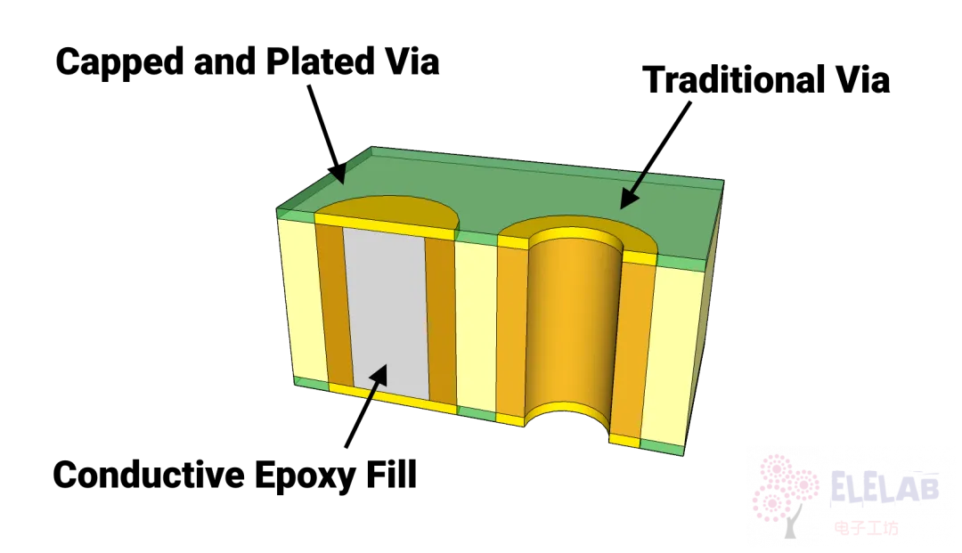
If there are hollow large vias and they undergo reflow soldering, the unfilled vias may be filled with solder. However, this can be interfered with by many factors, causing solder wicking, thus reducing the area of connection to the pads, leading to reliability issues. If the filled vias cannot be reliably grounded, it will affect thermal conductivity. The left figure below shows an example of an unfilled via after reflow, while the right shows an example of solder voids under the chip (indicated in red) that can be inspected with X-ray.
Voids increase the thermal interface’s thermal resistance. Similarly, excessive solder may cause the bottom of the board to be filled with protrusions, thus affecting the contact area between the board and the heat sink.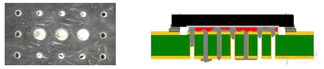
There are two methods to limit solder wicking. One method is to keep the via diameter less than 0.3mm. For smaller vias, the surface tension of the liquid solder inside the via better resists the gravitational effects on the solder. If the via structure is constructed according to the above guidelines, keeping the internal via diameter around 0.25mm to 0.3mm will minimize solder wicking. The downside of this method is that smaller openings lead to higher overall thermal resistance.
The other method to limit solder wicking involves using a solder mask layer to restrict solder from flowing from the top of the PCB to the bottom, referred to as a bottom via cap oil plug. This uses the solder mask layer to prevent solder from entering or leaving the thermal vias, depending on the side of the board where the solder mask is located (some may not cover well). A small area of solder mask can also be placed over the thermal vias on the top side of the PCB to prevent solder from flowing into the vias from the top side of the board. The left figure below shows a small hole with a complete LPI solder mask that protects the via. The right figure shows a via with a larger broken solder mask hole, which is due to the liquid nature of the LPI solder mask attempting to cover a hole that spans too large, resulting in solder leakage.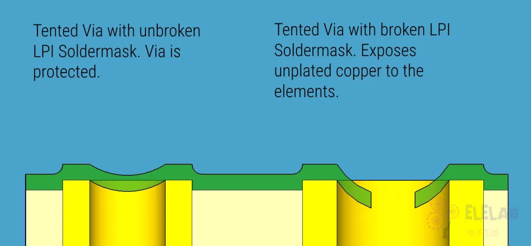
The following image shows the thermal resistance analysis results of FR-4 vias filled with materials of different conductivities, indicating that filled solid copper vias lead to lower thermal resistance, while unfilled vias provide higher thermal resistance. Vias filled with conductive epoxy perform slightly better than unfilled vias.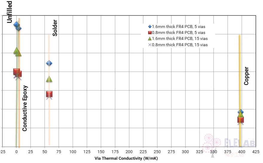
Impact of PCB Hole Diameter and Via Count
As explained in the previous section, the larger the solid hole, the lower the thermal resistance. However, we do not necessarily need to create solid copper filled vias, which can be costly. We have other methods to solve this problem, such as increasing the number of vias, which also shows significant improvement. The following simulation shows the relationship between via diameter and thermal resistance.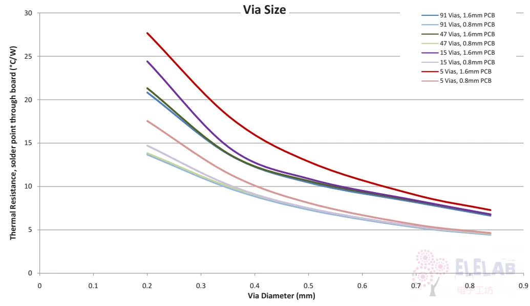 The next case considers the impact of changing the number of heat dissipation vias, as shown in the figure below. These vias are solid copper plated, with a diameter of 10mil and a center-to-center spacing of 25mil. This size was chosen because standard plating techniques can be used to fill the vias without additional processing. (14 vias represent the maximum area of the LED device heat sink pad).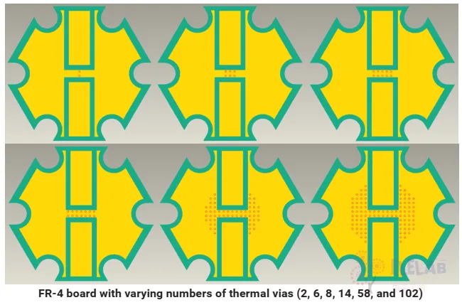
The results shown in the figure indicate that increasing the number of vias beyond 14 does not yield significant improvement (this is the maximum achievable density perpendicular to the LED heat sink pad).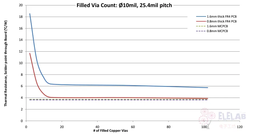
Given that the total available area for heat dissipation vias is typically fixed, it is advisable to use a larger number of smaller vias to fill a greater portion of that area. A 0.3mm hole is a reasonable size.
Impact of PCB Heat Dissipation Area
The following figure shows an FR-4 PCB with 14 copper plated vias of 0.254mm diameter, with the widths of the heat dissipation copper foil being (3.3, 4.0, 6.0, 10.0, 14.0, 20.0mm).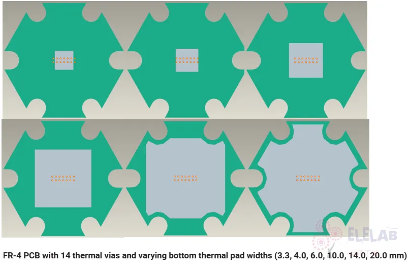
The simulation results in the figure show that as the width of the bottom thermal pad increases, there is a small difference in thermal resistance. For a board thickness of 1.6mm, increasing the width to over 12mm yields almost no improvement, while for a board thickness of 0.8mm, the improvement gradually decreases as the width exceeds 16mm.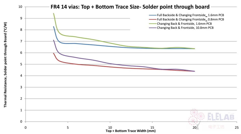
Summary of Thermal Simulation Results
The results of the simulation indicate that to minimize the thermal resistance of FR-4 boards, the dielectric thickness should be reduced to 0.8mm. While using a large number of vias can reduce thermal resistance, the cost of manufacturing the board also needs to be considered. Larger unfilled vias increase the likelihood of partial filling during soldering. Smaller solid filled vias are a better solution. Finally, due to thermal diffusion resistance, increasing additional vias and widening the area of copper foil beyond a certain point will diminish returns.It is recommended to create 10mil or 0.3mm (cost-effective) via areas. The reason for choosing this parameter is the combination of performance and manufacturability. According to several PCB manufacturers, using 10mil holes with a 25mil spacing is a reasonable and repeatable production option when used with 2oz. During the PCB plating process, solid copper can be reliably filled into the plating solution.The simulation shown in the last part regarding the impact of PCB hole diameter and via count indicates that on a 0.8mm FR-4 PCB, 10mil vias can achieve 4°C/W (via solid copper).Copyright Notice: This article is copyrighted by the original author and does not represent the views of the association. The articles promoted by the “Jiangxi Province Electronic Circuit Industry Association” are for sharing purposes only and do not represent the stance of this account. If there are copyright issues, please contact us for deletion.