PCB Panel Design: The Perfect Balance of Cost and Efficiency
In PCB manufacturing, panel design directly affects production efficiency and cost. A reasonable panel scheme can increase SMT placement efficiency several times, while incorrect designs can lead to reduced processing speed or even production failure. This article will delve into the core points of PCB panel design, helping you avoid common pitfalls and achieve efficient production!
1. Panel Size: Line Compatibility is Key1. Width Limitations: Conventional SMT production lines require a panel width of ≤260mm to 300mm (Figure 1). Exceeding this limit may cause the material gun to be incompatible, significantly reducing production efficiency.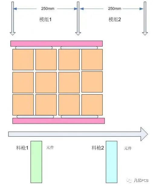 2. Frame Design:
- The clamping edges must have sufficient strength to avoid panel deformation.
- Do not create V-grooves on the clamping edges to ensure reliable fixture fixation.
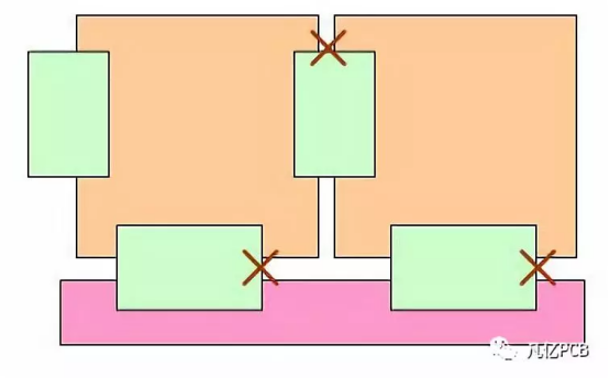
2. Component Layout: Orientation and Spacing Standards1. Unified Orientation Principle: All components must have a consistent orientation (Figure 2) to avoid mirrored layouts that can lead to coordinate positioning errors.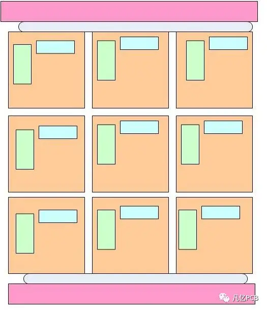 2. Edge Exclusion Rules:
- Devices such as connectors must not extend beyond the panel edges (Figure 3).
- The spacing between small boards must consider the operational space of the depaneling tools.
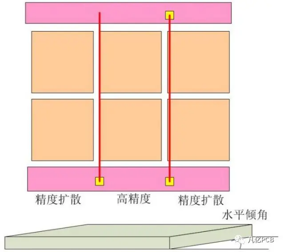
3. Positioning System: The Core of Precision Assurance1. Optical Positioning Points:
- Each panel must have at least 3 positioning points (Figure 4).
- Similar patterns are prohibited within a 1.5mm radius around the positioning points.
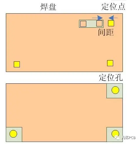
2. Mechanical Positioning Holes:
- Each small board must have at least 3 positioning holes (3mm ≤ hole diameter ≤ 6mm).
- Wiring or placement is prohibited within 1mm of the hole edges (Figure 5).
 4. Advanced Techniques: Details Determine Success or Failure1. Direction Marking: Set differentiated spacing along the edges of the panel in different travel directions (Figure 6) for quick identification.
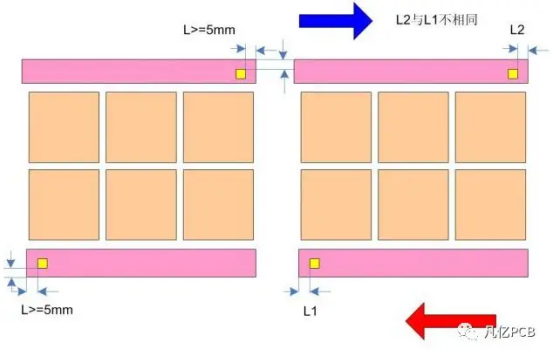 2. V-Groove Design:
- Depth should be controlled to 1/3 of the board thickness.
- Leave sufficient connection bridges (usually 0.5mm).
3. Stamping Hole Design:
- Applicable for irregular panel designs.
- Recommended hole diameter is 0.8-1.0mm.
5. Common Problems and Solutions
| Problem Phenomenon | Cause Analysis | Solution |
|---|---|---|
| SMT Placement Offset | Insufficient or obstructed positioning points | Increase the number of positioning points and ensure a clean surrounding area. |
| Difficulty in Depaneling | Connectors extending beyond the edge | Readjust the layout to leave sufficient depaneling space. |
| Panel Deformation | Improper design of clamping edges | Reinforce the clamping edges and avoid grooving. |
Conclusion: Golden Rules of Panel DesignStrictly follow production line specifications: Width ≤260mm to 300mm.Ensure reliable positioning: Dual assurance with optical points and mechanical holes.Optimize component layout: Unified orientation and edge avoidance.Consider subsequent processes: Reserve space for depaneling and testing.By following these key points, your panel design will meet the demands of both efficient production and cost control.
Want to learn more about PCB design?
Our modular courses will take you from beginner to expert!
—————————————————————————————This article is an original piece by Fanyi Education, please indicate the source when reprinting!For submissions/recruitment/advertising/course collaboration/resource exchange, please add WeChat: 13237418207
“Complete Guide to USB Interface PCB Design: Master Core Points from Type-C to High-Speed Routing in One Article!”
2025-04-30
11 Best Tips for High-Speed PCB Routing (Part 1)
2025-04-29
Design Specifications for Via in PCB Design: Balancing Performance and Cost
2025-04-28
[Hardcore Content] Comprehensive Analysis of DDR Module PCB Design: Topology, Routing Rules, and Error Control Must Not Be Missed!
2025-04-25