With a single FPGA, you can control arbitrary waveform generation, including frequency modulation and amplitude modulation! This project utilizes the DDS module and high-speed DAC in the “Little Foot” FPGA development board to achieve high-quality output of various waveforms such as sine, square, and triangle waves. The control method is very intuitive: switch waveform modes with buttons, use a rotary encoder to switch between “frequency modulation/amplitude modulation,” and then rotate for fine-tuning parameters. The entire system is logically clear and user-friendly, making it an excellent entry point for hardware enthusiasts to experience FPGA digital waveform synthesis.
1
Project Requirements

By using the high-speed DAC (10 bits/125 Msps) on the board in conjunction with the internal DDS logic of the FPGA, we can generate waveforms that are adjustable (sine, triangle, square), with adjustable frequency (DC-), and adjustable amplitude.
-
The frequency range of the generated analog signal is DC-20 MHz, with a tuning precision of 1 Hz.
-
The amplitude of the generated analog signal is up to 1 Vpp, with an adjustable range of 0.1 V to 1 V.
-
The onboard rotary encoder and buttons can be used to switch waveforms and adjust parameters.
2
Hardware Introduction

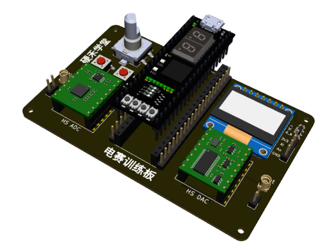
The development board used in this project is equipped with the “Little Foot” FPGA core board (fully FPGA solution) for electronic competition training:
The system block diagram is as follows:
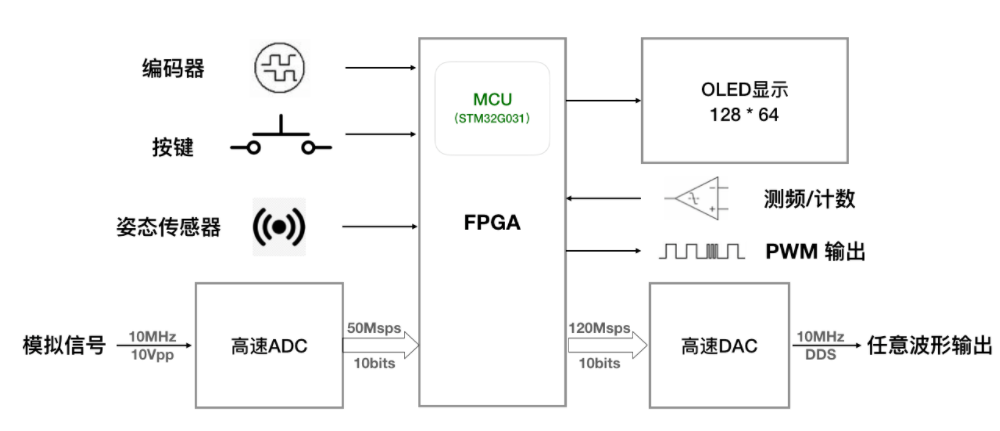
The functionalities used in the project include: encoder, buttons, high-speed DAC.
3
Completed Functions and Achieved Performance

1. Waveform Output
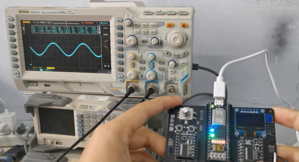
By using the onboard high-speed DAC to output arbitrary waveforms, the default is a sine wave, which can be observed by connecting the output pin to an oscilloscope.
2. Button Waveform Switching
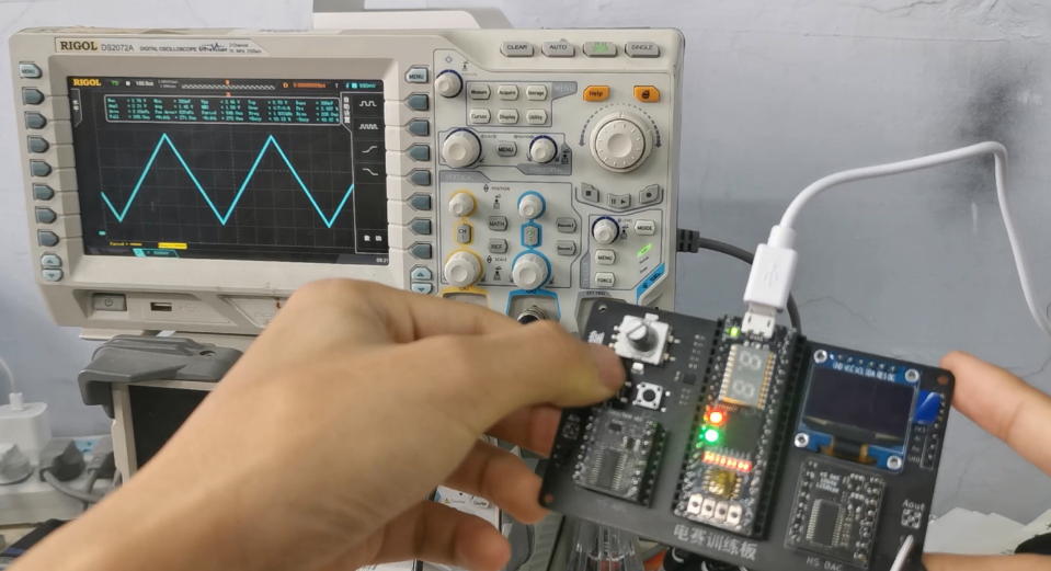
Waveforms can be switched using buttons K1 and K2 on the expansion board, currently allowing output of sine, triangle, and square waves.
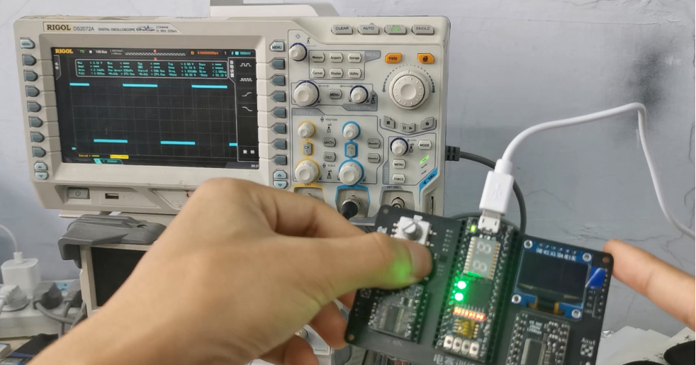
3. Encoder Frequency Modulation
Pressing the encoder switches between “frequency modulation/amplitude modulation mode,” allowing frequency adjustment of the output waveform by rotating the encoder left and right.
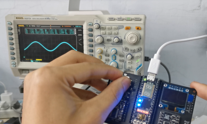
4. Encoder Amplitude Modulation
Pressing the encoder switches between “frequency modulation/amplitude modulation mode,” allowing amplitude adjustment of the output waveform by rotating the encoder left and right.

4
Implementation Approach

-
Use the built-in DDS logic of the FPGA to generate a 10-bit digital voltage signal, outputting it to the onboard high-speed DAC module, which outputs the corresponding waveform.
-
Set up a waveform state machine to manage the waveforms output by the FPGA, allowing switching between sine, square, and triangle waves via buttons.
-
Set up an encoder state machine to manage the current adjustment target of the encoder, allowing switching between frequency modulation and amplitude modulation via the encoder’s OK button.
5
Implementation Process

1. Program Architecture Diagram

(Note: The gray names in the lower right corner of each block diagram indicate the main functions executed by the files)
2. DDS Waveform Generation
The board is equipped with a 10-bit/120 Msps high-speed DAC, which generates a 10-bit digital voltage value through the internal DDS logic of the FPGA, outputting voltage data to the DAC module, which parses the data and outputs the corresponding waveform signal at the output pin.
To increase the maximum frequency of the generated waveform, the built-in phase-locked loop IP core of Diamond was used to multiply the 12 MHz clock signal to 120 MHz input to the DDS generation module, allowing the system to produce a maximum waveform signal of around 20 MHz. However, at around 20 MHz, there are only 6 sampling points per cycle, leading to significant distortion of the waveform.
For specific waveform generation, a 32-bit accumulator (referred to as cnt in the code) was defined, with the rising edge of the 120 MHz clock signal used to increment the accumulator. Both triangle and square waves can be directly obtained from the accumulator, with the triangle wave obtained as follows:
ori_out <= (cnt[31])?cnt[30:21]:~cnt[30:21];The square wave is obtained as follows:
ori_out <= {10{ cnt[31] }};The sine wave cannot be obtained through the accumulator; the project uses a lookup table method, calling the built-in sin-cos lookup table IP core of Diamond, inputting an 8-bit address and outputting 10-bit data.
//sin tablewire [9:0] dds_out_sin_temp;wire sin_clk_en = 1'b1;wire sin_reset = 1'b0;dds_sin_table u_dds_sin_table(.Clock(clk_pll), .ClkEn(sin_clk_en),.Reset(sin_reset),.Theta(cnt[31:24]),.Sine(dds_out_sin_temp));The DDS generation file (file: dds.v, called in: main.v):
module dds( input clk_pll, // Input clock input [2:0] wave_st, input [31:0] fm_step, input [7:0] am_factor, output reg [9:0]dds_out // Output set as reg to avoid glitches); // State machine parameter WAVE_STATE_SIN = 3'b110; // Sine wave parameter WAVE_STATE_SQUARE = 3'b101; // Square wave parameter WAVE_STATE_TRI = 3'b011; // Triangle wave // Amplitude modulation reg [17:0] am_out; // Original output reg [9:0] ori_out; // Accumulator reg [31:0] cnt; always @(posedge clk_pll) cnt <= cnt + fm_step; // Sin table wire [9:0] dds_out_sin_temp; wire sin_clk_en = 1'b1; wire sin_reset = 1'b0; dds_sin_table u_dds_sin_table( .Clock(clk_pll), .ClkEn(sin_clk_en), .Reset(sin_reset), .Theta(cnt[31:24]), .Sine(dds_out_sin_temp)); always @ (posedge clk_pll) begin case(wave_st) WAVE_STATE_SIN: ori_out <= dds_out_sin_temp + 10'd512; WAVE_STATE_SQUARE: ori_out <= {10{ cnt[31] }}; WAVE_STATE_TRI: ori_out <= (cnt[31])?cnt[30:21]:~cnt[30:21]; default: ori_out <= dds_out_sin_temp + 10'd512; endcase end // Amplitude modulation am_out <= ori_out * am_factor; dds_out <= am_out[17:8];endendmodule3. State Machine
The state machine is an important part of FPGA programming. Since the system needs to switch waveforms and adjust the amplitude and frequency of the waveforms, the system states are mainly divided into the current waveform type state and the encoder state, which are defined as follows:
// State machine waveparameter WAVE_STATE_SIN = 3'b110; // Sine waveparameter WAVE_STATE_SQUARE = 3'b101;// Square waveparameter WAVE_STATE_TRI = 3'b011; // Triangle wave reg [2:0] curr_wave_st; reg [2:0] next_wave_st; // State machine encparameter ENC_STATE_FM = 3'b110; // Frequency modulationparameter ENC_STATE_AM = 3'b101; // Amplitude modulation reg [2:0] curr_enc_st; reg [2:0] next_enc_st;For state switching, the system uses the left and right buttons to switch the waveform display, and the encoder OK button to switch between frequency modulation and amplitude modulation modes. The state switching code for the above two states is written in a three-part format to reduce code duplication, making it easier to manage and improving the stability of the timing logic.
The state switching code is as follows:
// First part: synchronous logic describing the transition from next state to current state always @ (posedge clk or negedge rst_n) begin if(!rst_n) curr_wave_st <= WAVE_STATE_SIN; else curr_wave_st <= next_wave_st; end // Second part: combinational logic describing the conditions for state transition always @ (curr_wave_st or rst_n or key_pulse) begin if(!rst_n) begin next_wave_st = WAVE_STATE_SIN; end else begin case(curr_wave_st) WAVE_STATE_SIN: begin if(key_pulse[0]) next_wave_st = WAVE_STATE_TRI; else if(key_pulse[1]) next_wave_st = WAVE_STATE_SQUARE; else next_wave_st = WAVE_STATE_SIN; end WAVE_STATE_SQUARE: begin if(key_pulse[0]) next_wave_st = WAVE_STATE_SIN; else if(key_pulse[1]) next_wave_st = WAVE_STATE_TRI; else next_wave_st = WAVE_STATE_SQUARE; end WAVE_STATE_TRI: begin if(key_pulse[0]) next_wave_st = WAVE_STATE_SQUARE; else if(key_pulse[1]) next_wave_st = WAVE_STATE_SIN; else next_wave_st = WAVE_STATE_TRI; end default: next_wave_st = WAVE_STATE_SIN; endcase end end // Third part: synchronous logic describing the output actions of the next state always @ (posedge clk or negedge rst_n) begin if(!rst_n==1) begin led_out[2:0] <= WAVE_STATE_SIN; end else begin case(next_wave_st) WAVE_STATE_SIN: begin led_out[2:0] <= WAVE_STATE_SIN; end WAVE_STATE_SQUARE: begin led_out[2:0] <= WAVE_STATE_SQUARE; end WAVE_STATE_TRI: begin led_out[2:0] <= WAVE_STATE_TRI; end default:begin led_out[2:0] <= WAVE_STATE_SIN; end endcase end end // Encoder state machine, same as above always @ (posedge clk or negedge rst_n) begin if(!rst_n) curr_enc_st <= ENC_STATE_FM; else curr_enc_st <= next_enc_st; end // Second part: combinational logic describing the conditions for state transition always @ (curr_enc_st or rst_n or enc_pulse_ok) begin if(!rst_n) begin next_enc_st = ENC_STATE_FM; end else begin case(curr_enc_st) ENC_STATE_FM: begin if(enc_pulse_ok) next_enc_st = ENC_STATE_AM; else next_enc_st = ENC_STATE_FM; end ENC_STATE_AM: begin if(enc_pulse_ok) next_enc_st = ENC_STATE_FM; else next_enc_st = ENC_STATE_AM; end default: next_enc_st = ENC_STATE_FM; endcase end end // Third part: synchronous logic describing the output actions of the next state always @ (posedge clk or negedge rst_n) begin if(!rst_n==1) begin led_out[5:3] <= ENC_STATE_FM; end else begin case(next_enc_st) ENC_STATE_FM: begin led_out[5:3] <= ENC_STATE_FM; end ENC_STATE_AM: begin led_out[5:3] <= ENC_STATE_AM; end default:begin led_out[5:3] <= ENC_STATE_FM; end endcase end end4. Button Debouncing and Encoder Decoding
The button debouncing and encoder decoding content references the code from the Electronic Forest, with the following URL:
-
Button Debouncing:
https://www.eetree.cn/wiki/7._%E6%8C%89%E9%94%AE%E6%B6%88%E6%8A%96
-
Encoder Decoding: [Rotary Encoder Module:
https://www.eetree.cn/wiki/%E6%97%8B%E8%BD%AC%E7%BC%96%E7%A0%81%E5%99%A8%E6%A8%A1%E5%9D%97]
In this, the button debouncing module can customize the number of buttons, and only one module instantiation is needed to achieve debouncing for multiple buttons.
5. Frequency Modulation and Amplitude Modulation
The principles of frequency modulation and amplitude modulation are referenced from the Electronic Forest’s DDS principle article: [dds_verilog:https://www.eetree.cn/wiki/dds_verilog]
Frequency modulation is achieved by changing the accumulation value of the DDS accumulator, while amplitude modulation is achieved by multiplying the generated waveform by a factor. For specifics, please refer to the articles linked above.
The accumulation value of the DDS accumulator is set to fm_step, and the amplitude modulation factor is set to am_factor. Two modules are defined to adjust these two values, and the adjusted parameters are input to the DDS waveform generation module through the top-level file main.v.
The code for frequency modulation is as follows:
module dds_fm(input clk, // Input clockinput rst_n,input enc_pulse_l,input enc_pulse_r,input [2:0] enc_st,output reg [31:0] dds_fm_step // Frequency modulation accumulation value);// State machineparameter ENC_STATE_FM = 3'b110; // Frequency modulationparameter ENC_STATE_AM = 3'b101; // Amplitude modulation// Frequency modulationalways @(posedge clk or negedge rst_n)beginif(!rst_n)dds_fm_step <= 32'h00_00_ff_ff;elsecase(enc_st)ENC_STATE_FM:if(enc_pulse_l)dds_fm_step <= dds_fm_step - 8'hff;else if(enc_pulse_r)dds_fm_step <= dds_fm_step + 8'hff;elsedds_fm_step <= dds_fm_step;default:dds_fm_step <= dds_fm_step;endcaseendendmoduleThe code for amplitude modulation is as follows:
module dds_am( input clk, // Input clock input rst_n, input enc_pulse_l, input enc_pulse_r, input [2:0] enc_st, output reg [7:0] dds_am_factor // Amplitude modulation factor);// State machineparameter ENC_STATE_FM = 3'b110; // Frequency modulationparameter ENC_STATE_AM = 3'b101; // Amplitude modulation// Amplitude modulationalways @(posedge clk or negedge rst_n) begin if(!rst_n) dds_am_factor <= 8'hff; else case(enc_st) ENC_STATE_AM: if(enc_pulse_l) dds_am_factor <= dds_am_factor - 8'h0f; else if(enc_pulse_r) dds_am_factor <= dds_am_factor + 8'h0f; else dds_am_factor <= dds_am_factor; default: dds_am_factor <= dds_am_factor; endcaseendendmodule6
Resource Report

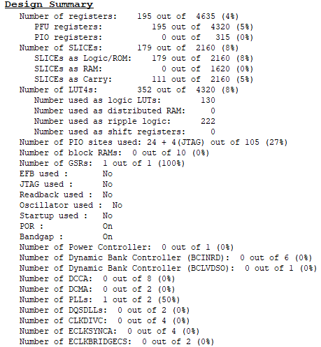
7
Main Challenges Encountered

1. Abnormal waveform from the built-in sin_table IP core
When generating DDS waveforms, the system calls the built-in IP core of Diamond as follows:
//sin tablewire [9:0] dds_out_sin_temp;wire sin_clk_en = 1'b1;wire sin_reset = 1'b0;dds_sin_table u_dds_sin_table(.Clock(clk_pll), .ClkEn(sin_clk_en),.Reset(sin_reset),.Theta(cnt[31:24]),.Sine(dds_out_sin_temp));However, the waveform obtained from this call is a strange waveform as shown in the following image:
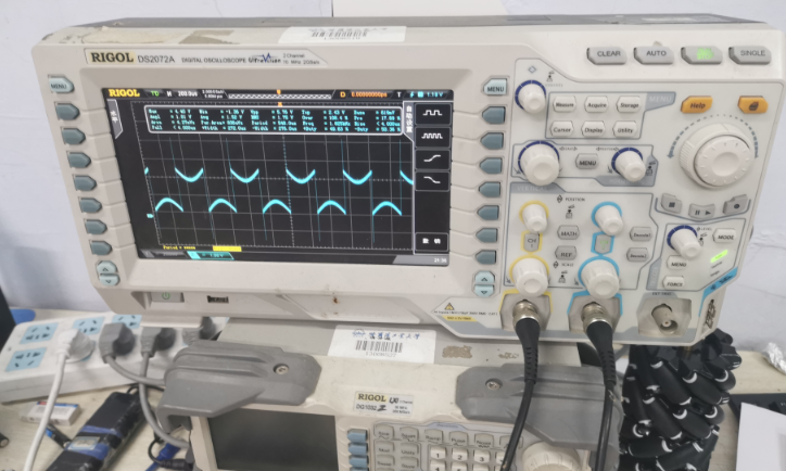
This is suspected to be due to an IP core setting issue or an internal logic error in the IP core. To generate a perfect sine wave, I added 10’d512 to the output wire of the sin_table, as follows:
ori_out <= dds_out_sin_temp + 10'd512;The resulting waveform is a perfect sine wave.
2. Difference between reg and wire
In the early stages of learning, I primarily used the default wire type and did not have a deep understanding of the differences between wire and reg. I mistakenly thought that wire and reg could not be assigned to each other, but through practice, I discovered that wire and reg can indeed be assigned to each other.
Since I initially used only wire, I could not assign values within always blocks, making it difficult to determine the waveform based on the state machine. In the three-way selection statement, I could only write it as follows:
assign dds_out =(wave_st == WAVE_STATE_SIN)? dds_out_sin:((wave_st == WAVE_STATE_SQUARE)?dds_out_square:dds_out_tri)This approach has poor readability and logic. Later, I changed dds_out and related variables to reg type, allowing the statement to determine the waveform type based on the state to be processed within the always block (see code in section 4.2), greatly improving code readability.
Additionally, tests showed that using reg instead of wire can also help reduce glitches.
8
Improvement Measures

This project has successfully implemented the functionality of a simple signal generator and achieved the expected indicators, but there are still many areas for improvement and expansion:
-
Utilize the onboard OLED to display waveforms and parameter lights, enhancing user interaction experience.
-
The use of buttons is not very sufficient; the complexity of the state machine can be increased to achieve bitwise adjustment of waveform frequency and amplitude.
-
Utilize the onboard ADC to implement a simple oscilloscope, linking it with the signal generator to form a complete system.

Click “Read the original text” to view the project