 Click the blue text above to follow me~Table of Contents4.
The Industrial Chain of Silicon Carbide
04The Industrial Chain of Silicon Carbide Devices
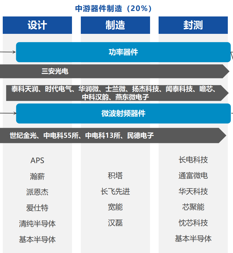
This article mainly discusses silicon carbide devices, which includedesign, manufacturing, and packaging and testing three major aspects.
01
Design
For silicon carbide devices, high-quality substrates can be purchased externally, and high-quality epitaxial wafers can also be sourced externally (the substrate and epitaxy will gradually mature and reduce in cost after large-scale stable production). However, this only provides a good foundation for obtaining a silicon carbide device. High-performance silicon carbide devices have extremely high requirements for the design and manufacturing processes, and design (similar to chip design) often plays the most decisive role.
Power MOSFETs are voltage-controlled devices with simple driving circuits, low driving power, and fast switching speeds, allowing for high operating frequencies.
Currently, the SiC industry has polarized: on one hand, there are conservative and safeplanar MOSFET designs, while on the other hand, there is a strong development of efficient and compacttrench MOSFET designs.
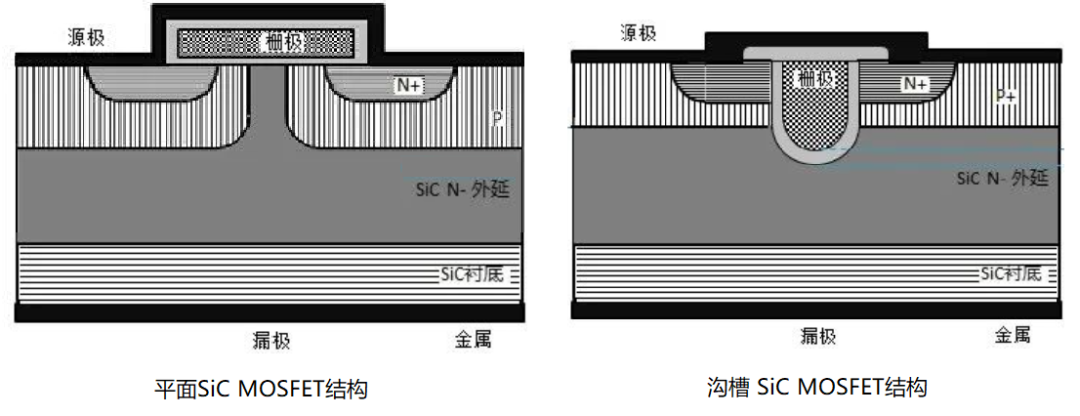
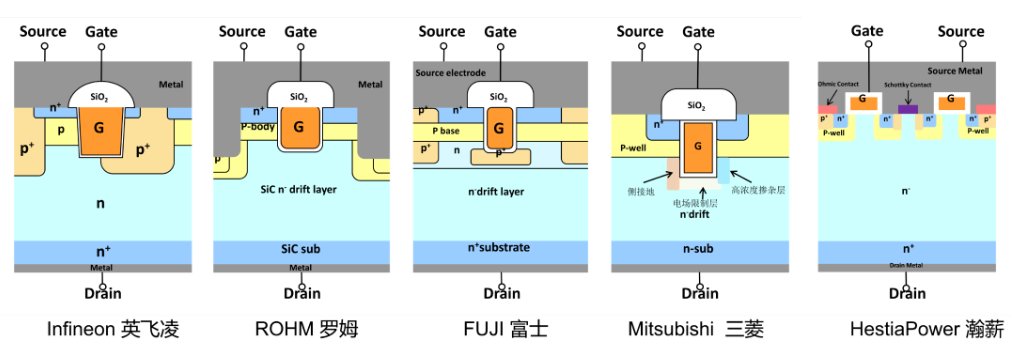
Until the end of 2023, there has been a divergence among the “Big Five” Western SiC device manufacturers. STMicroelectronics, ON Semiconductor, and Wolfspeed have been pursuing the traditional “planar” MOSFET architecture, while ROHM and Infineon are developing more complex trench MOSFET architectures.
Planar structures are characterized by simple processes, good unit consistency, and relatively high avalanche energy. However, this structure is prone to JFET effects, which increase on-state resistance and have larger parasitic capacitance.
– STMicroelectronics mainly focuses on planar structures, launching the fourth generation of planar gate silicon carbide, which began mass production in the second quarter of this year; compared to the previous generation, the fourth generation of planar gate silicon carbide has improved performance, including a 15% reduction in on-resistance and a doubling of the operating frequency to 1MHz.
– Wolfspeed’s silicon carbide MOSFETs adopt a planar design and are currently in the third generation (Gen 3), covering multiple voltage specifications from 650V to 1200V. The Gen 3 planar MOSFET features a hexagonal cell micro-design, with unit area on-resistances of 2.3 mΩ·cm2 for the 650V Gen 3 and 2.7 mΩ·cm2 for the 1200V Gen 3+, a 16% reduction compared to the previous generation Strip Cell. The Gen 4 trench gate is still under development, with no specific mass production timeline disclosed.
Trench structures embed the gate into the substrate, forming a vertical channel. Due to the need to create trenches, the process becomes complex, and unit consistency and avalanche energy are inferior to planar structures. However, this structure does not exhibit JFET effects, has a higher channel density, and the SiC crystal plane where the channel is located has a higher channel mobility, resulting in significantly lower on-resistance compared to planar junction structures; at the same time, parasitic capacitance is smaller, switching speeds are fast, and switching losses are very low. However, there are also significant issues: since the device operates under high voltage conditions, the internal electric field strength is high, especially at the bottom of the trench, where the electric field strength can easily exceed the maximum critical electric field strength, leading to local breakdown and affecting the reliability of the device’s operation.
– Infineon’s CoolSiC™ MOSFET adopts an asymmetric trench structure, where the MOS channel is oriented in the most favorable direction.
– ROHM has developed a third-generation product – a dual trench MOSFET structure, which features both source trench and gate trench.
In summary, in terms of performance, planar structures are certainly inferior to trench structures, but planar structures still have reliability advantages. Currently, trench structures still face significant challenges in manufacturing processes. However, the future evolution of trench technology is continuously addressing this issue, and more manufacturers are focusing their R&D efforts on trench structures, primarily to solve reliability issues, which essentially boils down to “how to reduce the electric field strength at the bottom of the trench”.
02
Manufacturing
The manufacturing process of silicon carbide devices is generally similar to that of silicon-based devices, mainly including processes such as photolithography, cleaning, doping, etching, film deposition, and thinning.
The unique properties of silicon carbide materials dictate that certain processes in device manufacturing require specific equipment for special development to enable silicon carbide devices to withstand high voltage and high current functions, mainly covering doping, gate structure formation, morphology etching, metalization, and thinning processes.
❶ Doping and Annealing
In the doping step, traditional silicon power device processes mainly use high-temperature diffusion and ion implantation as the primary doping control methods, each with its advantages and disadvantages, which will not be elaborated here.
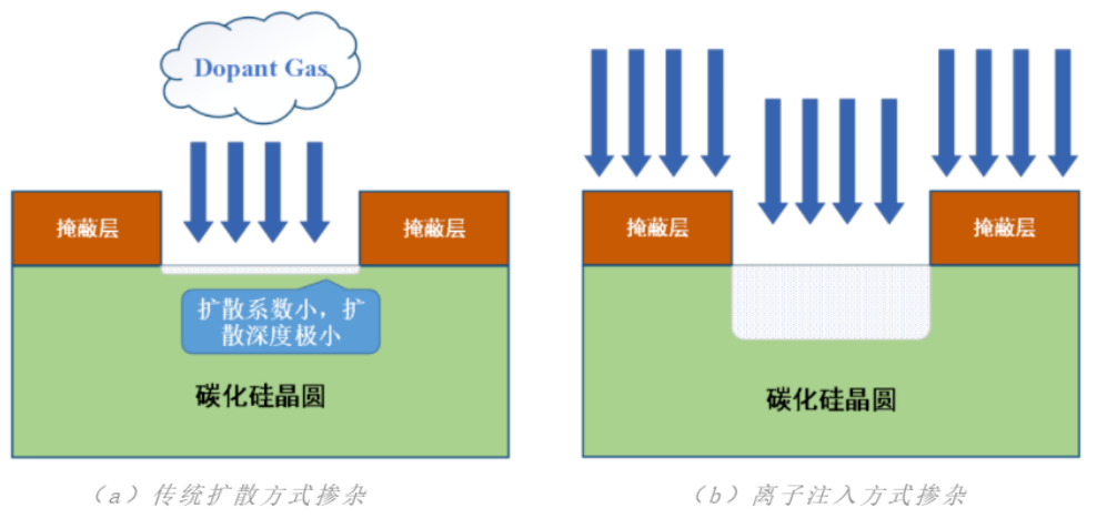
In the doping process of silicon carbide power devices, commonly used doping elements include: N-type doping, mainly nitrogen and phosphorus; P-type doping, mainly aluminum and boron. The diffusion coefficients of doping elements in silicon are relatively high, so high-temperature diffusion doping can be achieved at around 1300°C. Compared to the diffusion coefficients in silicon, phosphorus, aluminum, boron, and nitrogen have very low diffusion coefficients in silicon carbide, requiring temperatures above 2000°C to achieve reasonable diffusion coefficients.
However, high-temperature diffusion can introduce many issues, such as various diffusion defects that degrade the electrical performance of the device, and the inability to use common photoresists as masks, etc. Therefore, ion implantation has become the only choice for doping in silicon carbide.
After high-temperature ion implantation, the original lattice structure of silicon carbide is damaged and becomes amorphous. This lattice damage must be repaired during the annealing process to restore it to a single crystal structure and activate the dopants.
During the high-temperature annealing process, atoms can gain energy from thermal energy and undergo rapid thermal motion. When they move to positions in the single crystal lattice with the lowest free energy, they will remain in those positions. Thus, the damaged amorphous silicon carbide and dopant atoms will complete the construction of the single crystal structure by falling into lattice positions and being bound by lattice energy near the substrate interface. This lattice repair and activation rate improvement occur simultaneously during the annealing process. If the annealing temperature is 1400°C, the activation rate is less than 10%; generally, it needs to reach as high as 1600°C to achieve a 90% activation rate.
The processes of ion implantation and activation annealing are highly challenging, and various defects that inevitably arise can degrade device performance. Therefore, the requirement to control defects and improve yield undoubtedly poses significant challenges for equipment and process control.
Thus, whether one possesses high-temperature high-energy ion implantation machines has become one of the important standards for evaluating silicon carbide production lines.
Currently, high-temperature high-energy ion implantation machines are mainly monopolized by American manufacturers, with Applied Materials and Axcelis together accounting for over 70% of the global market. It is reported that ShuoKe ZhongKe Xin is currently the only domestic company that can provide this equipment, with a localization rate of 100%, maintaining the top market share in the domestic market. In terms of high-temperature annealing furnaces, major foreign manufacturers include Centrotherm and Japan Vacuum, while domestic manufacturers include North Huachuang, China Electronics Technology Group 48th Institute, and Yitang Semiconductor.
❷ Gate Structure Formation
The quality of the SiC/SiO2 interface significantly affects the channel mobility of MOSFETs and gate reliability, necessitating the development of specific gate oxides and post-oxidation annealing processes to compensate for dangling bonds at the SiC/SiO2 interface with special atoms (e.g., nitrogen atoms), meeting the performance requirements for high-quality SiC/SiO2 interfaces and high mobility devices. The core processes include high-temperature oxidation of gate oxides, LPCVD, and PECVD.

Diagram of ordinary oxide film deposition and high-temperature oxidation
❸ Morphology Etching
Silicon carbide materials exhibit inertness in chemical solvents, and precise morphology control can only be achieved through dry etching methods; the selection of mask materials, mask etching, mixed gases, sidewall control, etching rates, and sidewall roughness all need to be developed based on the characteristics of silicon carbide materials. The core processes include thin film deposition, photolithography, dielectric film etching, and dry etching processes.
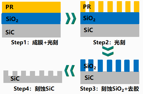
Diagram of the silicon carbide etching process
❹ Metalization
The source electrode of the device requires good low-resistance ohmic contact with silicon carbide. This not only requires controlling the metal deposition process and the interface state of the metal-semiconductor contact but also requires high-temperature annealing to reduce the Schottky barrier height and achieve metal-silicon carbide ohmic contact. The core processes are metal magnetron sputtering, electron beam evaporation, and rapid thermal annealing.
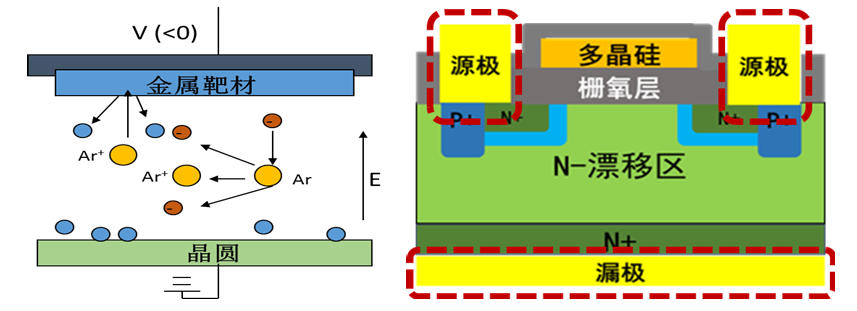
Diagram of magnetron sputtering principle and metalization effect
❺ Thinning Process
Silicon carbide materials have high hardness, high brittleness, and low fracture toughness, making them prone to brittle fracture during grinding processes, causing damage to the wafer surface and subsurface. New grinding processes need to be developed to meet the manufacturing needs of silicon carbide devices. The core processes include wafer thinning, film attachment, and film removal.
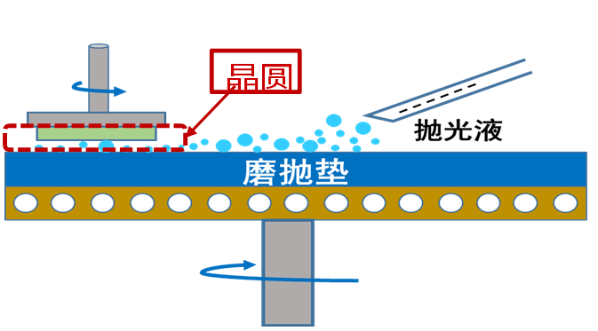
Diagram of wafer grinding/polishing/thinning principle
03
Packaging and Testing
The excellent characteristics of silicon carbide chips need to be realized through packaging and circuit systems to achieve efficient and reliable power connections.
Currently, the new design direction for SiC modules is to be more compact, utilizing double-sided silver sintering and copper wire bonding technologies, as well as high-performance silicon nitride AMB ceramic boards, liquid-cooled copper-based PinFin boards, and multi-signal monitoring induction terminals (compatible with welding and crimping) designs, striving for low loss, high blocking voltage, low on-resistance, high current density, and high reliability.
Currently, innovations in silicon carbide power module packaging are mainly moving in the following directions:
– More advanced connection materials and processes to withstand higher temperature variations
AI2O3-DBC has the highest thermal resistance but the lowest manufacturing cost; AlN-DBC has the lowest thermal resistance but poor toughness; Si4N3-AMB ceramic materials have medium thermal resistance, excellent toughness, and superior thermal capacity parameters, significantly enhancing the module’s heat dissipation capability, current capacity, and power density. Its thermal expansion coefficient is closer to that of the third-generation semiconductor substrate SiC crystal material, making it more stable and suitable for automotive-grade silicon carbide module applications. AMB ceramic substrates are expected to become a new trend in the IGBT and SiC device fields.
– Shorter connection paths and more advanced connection technologies to reduce parasitics to adapt to the high-frequency characteristics of devices
Silver sintering is currently the most advanced welding technology in the silicon carbide module field, fully meeting the stringent requirements of automotive-grade power modules for high and low-temperature operating scenarios. Compared to traditional tin soldering technology, silver sintering can achieve zero voids, low-temperature sintering for high-temperature service, and a reduction in solder layer thickness by 60-70%, making it suitable for high-temperature device interconnections, with electrical and thermal performance superior to tin solder, with conductivity increased by 5-6 times and thermal conductivity increased by 3-4 times.
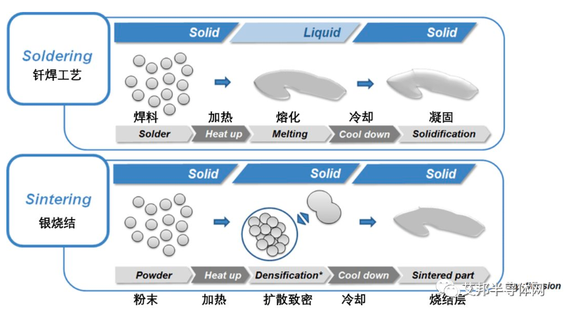
– More integrated packaging structure designs and circuit topologies for better system thermal management
To make the thermal path design of module products more compact, promoting more compact and efficient inverter system integration design, further reducing overall system inverter costs, changes in packaging forms improve heat dissipation and current-carrying capacity. The internal structure adopts multi-chip parallel configurations, with parameters of each parallel main circuit and drive circuit being basically consistent, maximizing the current-sharing of parallel chips. The module is internally packaged with temperature sensors (PTC), and the PTC is installed in the center of the module close to the chip, achieving tight thermal coupling for accurate temperature measurement of the module.
This article was mainly written with reference to the following public accounts and materials, and I would like to thank them for the self-learning process:Power Semiconductor Home, Silicon Carbide Research Society, NE Times Semiconductor, Smart Semiconductor, Haogao Electronic Technology, Aibang Semiconductor Network etc.
To be continued, please stay tuned.
 VCJinshuihe
Anchored in terminal application scenarios
Long-term deep cultivation in advanced new materials industry investment
◆ ◆ ◆ ◆ ◆ ◆ ◆ ◆ END ◆ ◆ ◆ ◆ ◆ ◆ ◆ ◆
Copyright Statement:
This public account is a learning and communication platform aimed at personal originality and knowledge sharing. Some content is original, while other content is sourced from the internet or reprinted from public accounts. I cannot provide any explicit or implicit guarantees regarding the accuracy, reliability, or completeness of the content, even if I agree with the views expressed in the text. Please use it for learning reference only. I highly respect the achievements and contributions of the authors. If there is any infringement, please contact me for timely deletion.