Source: Content from “CITIC Securities Xu Tao, Hu Ye Qian Wen, and Yan Lei”, thank you.
Wafers (wafer) are the fundamental raw materials for manufacturing semiconductor devices. Extremely high-purity semiconductors are prepared into wafers through processes such as crystal pulling and slicing. Wafers undergo a series of semiconductor manufacturing processes to form extremely small circuit structures, and then they are cut, packaged, and tested to become chips, which are widely used in various electronic devices. The materials for wafers have undergone over 60 years of technological evolution and industrial development, resulting in today’s industry landscape dominated by silicon, supplemented by new semiconductor materials.
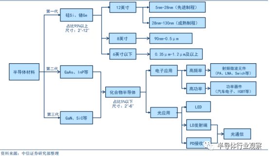
Basic Framework of Semiconductor Wafer Materials
In the 1950s, germanium (Ge) was the earliest semiconductor material used, initially in discrete devices. The invention of integrated circuits was an important step forward for the semiconductor industry. In July 1958, at Texas Instruments in Dallas, Jack Kilby manufactured the first integrated circuit using a piece of germanium semiconductor material as the substrate.
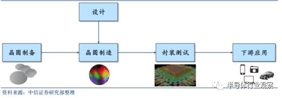
Semiconductor Industry Chain Process
However, germanium devices have shortcomings in high-temperature resistance and radiation resistance, and by the late 1960s, they were gradually replaced by silicon (Si) devices. Silicon is extremely abundant, and its purification and crystallization processes are mature. The silicon dioxide (SiO2) thin film formed by oxidation has good insulation properties, greatly improving the stability and reliability of devices. Therefore, silicon has become the most widely used semiconductor material. In terms of semiconductor device output, over 95% of semiconductor devices and over 99% of integrated circuits worldwide use silicon as the substrate material.
In 2017, the global semiconductor market size was approximately $412.2 billion, while the compound semiconductor market size was about $20 billion, accounting for less than 5%. In terms of wafer substrate market size, the annual sales of silicon substrates in 2017 were $8.7 billion, GaAs substrates about $800 million, GaN substrates about $100 million, and SiC substrates about $300 million. Sales of silicon substrates accounted for over 85%. In the 21st century, its dominant and core position will remain unshaken. However, the physical properties of Si materials limit their application in optoelectronics and high-frequency, high-power devices.
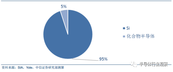
Semiconductor Market Share (by Material)
Since the 1990s, second-generation semiconductor materials represented by gallium arsenide (GaAs) and indium phosphide (InP) have begun to emerge. Materials like GaAs and InP are suitable for making high-speed, high-frequency, high-power, and optoelectronic devices, and are excellent materials for making high-performance microwave, millimeter-wave devices, and optoelectronic devices, widely used in satellite communications, mobile communications, optical communications, GPS navigation, and other fields. However, GaAs and InP materials are scarce, expensive, and toxic, which can pollute the environment. InP is even considered a suspected carcinogen, which limits the application of second-generation semiconductor materials significantly.
Third-generation semiconductor materials mainly include SiC and GaN, which are also known as wide bandgap semiconductor materials due to their bandgap width (Eg) being greater than or equal to 2.3 electron volts (eV). Compared to first and second-generation semiconductor materials, third-generation semiconductor materials have advantages such as high thermal conductivity, high breakdown field strength, high saturation electron drift velocity, and high bond energy, which can meet the new requirements of modern electronic technology for high temperature, high power, high voltage, high frequency, and radiation resistance in harsh conditions. They are the most promising materials in the field of semiconductor materials, with important application prospects in defense, aviation, aerospace, oil exploration, optical storage, etc. In many strategic industries such as broadband communications, solar energy, automobile manufacturing, semiconductor lighting, and smart grids, they can reduce energy loss by more than 50%, and can reduce the size of equipment by more than 75%, which has milestone significance for the development of human technology.
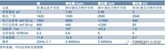
Comparison of Wafer Material Properties
Compound semiconductors are semiconductor materials formed by two or more elements. Most second and third-generation semiconductors belong to this category. According to the number of elements, they can be divided into binary compounds, ternary compounds, quaternary compounds, etc. Binary compound semiconductors can also be classified based on the position of their constituent elements in the periodic table into III-V group, IV-IV group, II-VI group, etc. Compound semiconductor materials represented by gallium arsenide (GaAs), gallium nitride (GaN), and silicon carbide (SiC) have become the fastest developing, most widely used, and largest volume semiconductor materials after silicon.
Compound semiconductor materials have superior performance and energy band structures:
(1) High electron mobility;
(2) High frequency characteristics;
(3) Wide frequency bandwidth;
(4) High linearity;
(5) High power;
(6) Material selection diversity;
(7) Radiation resistance.
Therefore, compound semiconductors are mainly used in the manufacturing of RF devices, optoelectronic devices, power devices, etc., and have great development potential; silicon devices are mainly used in logic devices, memory, etc., and they are irreplaceable in each other.
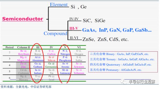
Compound Semiconductor Materials
Wafer Preparation: Substrate and Epitaxy Process
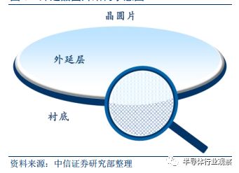
Wafer preparation includes two major steps: substrate preparation and epitaxy process. The substrate is a wafer slice made of single-crystal semiconductor material. The substrate can directly enter the wafer manufacturing stage to produce semiconductor devices or can undergo epitaxy processing to produce epitaxial wafers. Epitaxy refers to the process of growing a new single crystal on a single crystal substrate, where the new single crystal can be the same material as the substrate or a different material. Epitaxy can produce a wider variety of materials, providing more choices for device design.
The basic steps of substrate preparation are as follows: Semiconductor polycrystalline materials are first purified, doped, and pulled to obtain single-crystal materials. Taking silicon as an example, silicon sand is first refined and reduced to metallurgical-grade rough silicon with a purity of about 98%. After multiple purifications, electronic-grade high-purity polysilicon is obtained (purity reaches 99.9999999% or more, 9-11 nines). Single-crystal silicon rods are obtained through furnace pulling. Single-crystal materials undergo mechanical processing, chemical treatment, surface polishing, and quality inspection to obtain single-crystal polished slices that meet certain standards (thickness, crystal orientation, flatness, parallelism, and damage layer). The purpose of polishing is to further remove the residual damage layer on the processed surface. The polished slices can be directly used to make devices or can be used as substrate materials for epitaxy.
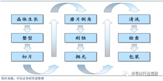
Basic Steps of Substrate Preparation
The epitaxy growth process currently mainly includes two technologies: MOCVD (Metal-Organic Chemical Vapor Deposition) and MBE (Molecular Beam Epitaxy). For example, Allnew Optoelectronics uses MOCVD, while Epistar uses MBE technology.
Comparison of MBE and MOCVD Technologies
Wafer Size: Varying Technological Development Processes
Silicon wafers can reach a maximum size of 12 inches, while compound semiconductor wafers can reach a maximum of 6 inches. The mainstream size for silicon wafer substrates is 12 inches, accounting for about 65% of global silicon wafer production capacity. 8 inches is also a commonly used mature process wafer, accounting for 25% of global production capacity. The mainstream sizes for GaAs substrates are 4 inches and 6 inches; SiC substrates are mainly supplied in sizes of 2 inches and 4 inches; GaN self-supporting substrates are mainly 2 inches.
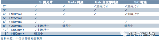
Substrate Wafer Material Corresponding Sizes
Currently, SiC substrates have reached a size of 6 inches, and 8 inches are under development (II-VI has manufactured samples). However, the mainstream still uses 4-inch wafers. The main reasons are (1) Currently, 6-inch SiC wafers cost about 2.25 times that of 4-inch wafers. By 2020, this is expected to be about 2 times, and there has not been significant progress in cost reduction. Additionally, changing equipment requires extra capital expenditure, and the advantage of 6 inches is only in production efficiency; (2) The quality of 6-inch SiC wafers is lower than that of 4-inch wafers, and therefore, 6 inches are mainly used to manufacture diodes, as manufacturing diodes on lower quality wafers is simpler than on MOSFETs.
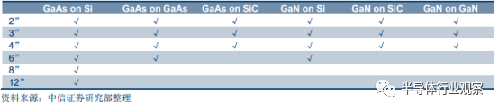
Corresponding Wafer Sizes for Epitaxy Growth
GaN materials lack single-crystal materials in nature, so they have long been epitaxially grown on heterogeneous substrates such as sapphire, SiC, and Si. Nowadays, 2-inch, 3-inch, and 4-inch GaN self-supporting substrates can be produced through hydride vapor phase epitaxy (HVPE) and ammonothermal methods. Currently, in commercial applications, GaN epitaxy on heterogeneous substrates is still dominant, while GaN self-supporting substrates have the greatest application in lasers, achieving higher luminous efficiency and quality.
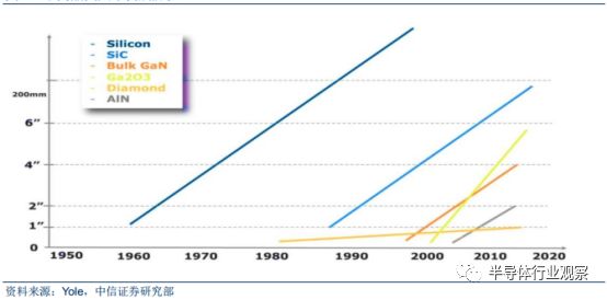
Development History of Different Wafer Sizes
Silicon: Mainstream Market with Strong Demand in Niche Areas
From the perspective of silicon wafer supply manufacturers: Japanese manufacturers control the market with a stable oligopoly. Japanese manufacturers occupy over 50% of the silicon wafer market share. The top five manufacturers account for over 90% of the global share. Among them, Shin-Etsu Chemical of Japan accounts for 27%, SUMCO of Japan 26%, with these two companies combined accounting for 53%, more than half. Taiwan’s GlobalWafers acquired SunEdison Semiconductor during the downturn of the wafer industry in December 2016, moving from sixth to third place, with a share of 17%. Germany’s Siltronic accounts for 13%, and Korea’s SK Siltron (formerly LG Siltron, acquired by SK Group in 2017) accounts for 9%. Unlike the top four manufacturers, SK Siltron only supplies Korean customers.
Additionally, there are companies such as Soitec from France, TSMC from Taiwan, and others with relatively small shares. The various major manufacturers differ in the types and sizes of wafers they supply. Overall, the top three manufacturers have more diverse products. The top three manufacturers can supply Si annealed wafers and SOI wafers, with only Shin-Etsu being able to supply 12-inch SOI wafers. Germany’s Siltronic and Korea’s SK Siltron do not provide SOI wafers, and SK Siltron does not supply Si annealed wafers. However, there is basically no difference in size for Si polished wafers and Si epitaxial wafers among various manufacturers.
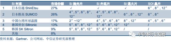
Competitiveness of Silicon Wafer Suppliers
For the past 15 years, Japanese manufacturers have consistently held over 50% of the silicon wafer market share. There has not been a significant regional transfer of silicon wafer production capacity. According to Gartner, in 2007, the market share of silicon wafers was led by Japan’s Shin-Etsu (32.5%), followed by Japan’s SUMCO (21.7%), and Germany’s Siltronic (14.8%); in 2002, the market share was led by Shin-Etsu (28.9%), SUMCO (23.3%), and Siltronic (15.4%). A significant recent market change was Taiwan’s GlobalWafers acquiring SunEdison in December 2016, moving from the sixth to the third largest manufacturer. However, Japanese manufacturers have always held over 50% of the market share.
Japan’s competitiveness in the fab segment has declined, while it has maintained a leading position in the materials segment. In the mid-1980s, Japan’s semiconductor industry once held over 50% of the world’s share. Japan’s advantage in semiconductor materials has continued since last century, while its competitiveness in wafer manufacturing has significantly weakened, with a clear regional shift in the semiconductor fab segment. The reasons are that the fab segment is closer to the demand side and experiences greater market fluctuations; however, silicon wafers are highly homogeneous, and new entrants need a considerable amount of time to validate their products with customers; moreover, wafers account for less than 10% of the cost in wafer foundries, and foundries are reluctant to risk changing to unproven products for minor price differences.
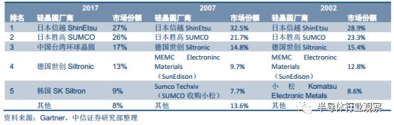
Changes in Silicon Wafer Supplier Shares Over the Past 15 Years
Silicon Wafer Demand Supplier Landscape: Mainly Overseas, Domestic Manufacturers Have Their Highlights
In IC design, major players dominate with high competition barriers, and since 2018, AI chips have become a new growth driver. Qualcomm, Broadcom, MediaTek, Apple, and other manufacturers are the strongest, while domestic manufacturer HiSilicon has risen. With the development of technology leading to upgrades in terminal products, the demand for IC products for innovative applications such as AI chips is continuously expanding. It is expected that by 2020, the market size for AI chips will grow from about $600 million in 2016 to $2.6 billion, with a CAGR of 43.9%. Currently, both domestic and foreign IC design manufacturers are actively laying out the AI chip industry. NVIDIA is the leader in the AI chip market, while AMD and Tesla are jointly developing AI chips for autonomous driving.
For domestic manufacturers, HiSilicon was the first to launch the Kirin 970 AI chip in September 2017, which has been successfully integrated into models such as the P20; Bitmain’s BM1680, the world’s first tensor acceleration computing chip, has been successfully applied in Bitcoin mining machines; Cambricon’s 1A processor, Horizon’s Journey, and Sunrise processors have also emerged. IC design oriented towards terminals and markets has become inevitable, and domestic manufacturers have significant advantages. The IC design industry is demand-driven, which can better serve downstream customers. Manufacturers of mobile processing chips and baseband chips like HiSilicon and Spreadtrum have rapidly risen to the top ten global IC design companies due to the explosive growth of the Chinese smartphone market in recent years. HiSilicon chips have been fully applied in Huawei smartphones, while manufacturers like Samsung and Xiaomi have also adopted self-developed chips. Currently, China is the largest terminal demand market globally, thus domestic IC design has a significant development advantage.
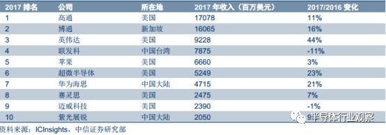
Global IC Design Manufacturers Ranking in 2017
In terms of foundry manufacturing, manufacturers’ Capex is growing rapidly, led by giants like Samsung and TSMC. In terms of capital expenditure, the competition in the global advanced process chip market is fierce, with the top three chip manufacturers, Samsung, Intel, and TSMC, each reaching a Capex of over $10 billion, with 2017 figures of $44 billion, $12 billion, and $10.8 billion, respectively. It is expected that Samsung’s total Capex will approach $110 billion over the next three years, while Intel and TSMC’s Capex in 2018 is expected to reach $14 billion and $12 billion, respectively, both showing significant growth, benefiting the giants in capturing the market through advanced process technology development and production line expansion.
In terms of process technology, TSMC is leading the industry and has already mass-produced 10nm process chips, with 7nm process expected to enter mass production in 2018; the most advanced foundry in mainland China, SMIC, currently has the capability for 28nm process mass production, while TSMC had already achieved 28nm mass production capability as early as 2011. In comparison, mainland manufacturers still have a significant gap.
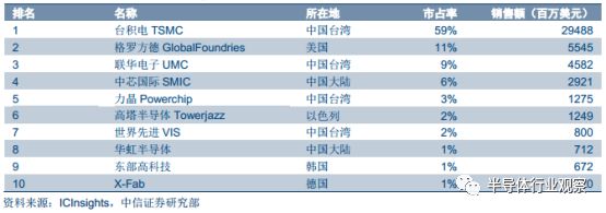
Global Pure-Play Wafer Foundry Manufacturers Ranking in 2016
In terms of packaging and testing, the trend of high-end manufacturing + packaging and testing integration is becoming apparent, with domestic manufacturers narrowing the technology gap with Taiwanese manufacturers. Packaging and testing technology has developed through four generations, and in the highest-end technology, manufacturing and packaging have achieved integration, with TSMC establishing two major high-level packaging ecosystems, CoWoS and InFO, and planning to double InFO capacity to meet the demand for Apple’s A12 chip.
Leading packaging manufacturer ASE has mastered top-notch packaging and microelectronics manufacturing technology, being the first to mass-produce TSV/2.5D/3D related products, and in March 2018, formed a joint venture with Japanese company TDK to expand SiP layout. Due to the relatively low technical barriers of packaging technology, domestic manufacturers are rapidly catching up, and the technology gap with global leaders is gradually narrowing. Domestic manufacturers have basically mastered advanced technologies such as SiP, WLCSP, and FOWLP, and applications such as FC and SiP packaging technologies have achieved mass production.
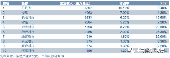
Global Semiconductor Packaging Manufacturers Ranking in 2017
A new round of regional transfer is aimed at mainland China. Although the top IC design, manufacturing, and packaging manufacturers are currently mainly located in the US and Taiwan, overall, the semiconductor manufacturing industry has undergone a historical development process from the US to Japan and then to Korea and Taiwan: In the 1950s, the semiconductor industry originated in the US, with the transistor invented in 1947 and the integrated circuit born in 1958. In the 1970s, semiconductor manufacturing shifted from the US to Japan. DRAM was an important entry point for the development of the industry in Japan and South Korea, and by the 1980s, Japan had taken the lead in the semiconductor industry. In the 1990s, with DRAM as the opportunity, the industry shifted to Korean manufacturers like Samsung and Hynix, while the wafer foundry segment shifted to Taiwan, where TSMC and UMC emerged. In the 2010s, the smartphone and mobile internet exploded, and industries such as IoT, big data, cloud computing, and artificial intelligence grew rapidly. The demographic dividend and demand transfer may drive manufacturing transfer, and it can be foreseen that mainland China has become the destination for a new round of regional transfer.
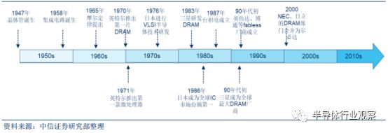
History of Regional Transfer in the Global Semiconductor Industry: US-Japan-Korea
Silicon Wafer Downstream Application Split: Size and Process Drive Technological Progress
Wafer size and process technology develop in parallel, with each process stage corresponding to a wafer size. (1) Process advancement → transistor miniaturization → transistor density increases exponentially → performance improvement. (2) Increasing wafer size → more chips produced per wafer → efficiency improvement → cost reduction. Currently, production equipment for 6-inch and 8-inch silicon wafers has generally completed depreciation, resulting in lower production costs, mainly producing mature processes above 90nm. Some processes have outputs on wafers of adjacent sizes. 5nm to 0.13μm uses 12-inch wafers, with 28nm serving as the boundary that distinguishes advanced processes from mature processes. The main reason is that after 28nm, new designs and processes such as FinFET are introduced, greatly increasing the difficulty of wafer manufacturing.
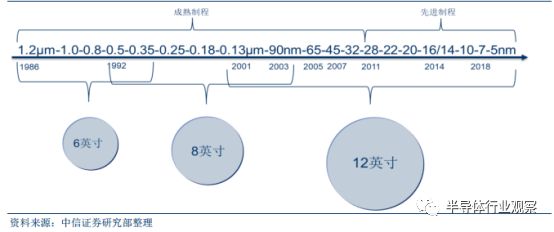
Silicon Wafer Size and Process Correspondence
In terms of total wafer demand, the 12-inch NAND and 8-inch markets are the core driving forces. The demand for 12-inch silicon wafers for storage accounts for 35%, the largest share, followed by 8-inch and 12-inch logic. In terms of sales revenue, among global integrated circuit products, memory accounts for about 27.8%, logic circuits account for 33%, microprocessor chips and analog circuits account for 21.9% and 17.3%, respectively. According to our forecasts, global demand for 12-inch silicon wafers in the second half of 2016 was about 5.1 million pieces per month, with demand for logic chips at 1.3 million pieces per month, DRAM demand at 1.2 million pieces per month, NAND demand at 1.6 million pieces per month, and other demands including NOR Flash, CIS, etc. at 1 million pieces per month; 8-inch silicon wafer demand was 4.8 million pieces per month, which, when converted to 12-inch wafers, is about 2.13 million pieces per month, with demand for wafers below 6 inches equivalent to about 620,000 pieces per month.
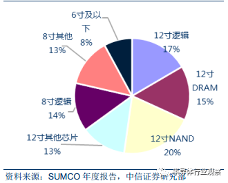
12-inch, 8-inch, and 6-inch Wafer Demand Structure
Thus, it is estimated that the demand for 12-inch wafers for storage, including NAND and DRAM, accounts for about 35% of total demand, while the demand for 8-inch wafers accounts for about 27%, and the demand for 12-inch wafers for logic chips accounts for about 17%. In terms of demand, currently, memory contributes the most to wafer demand, followed by mid-to-low-end applications for 8-inch wafers.
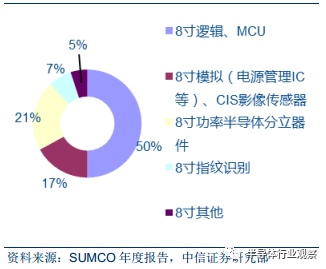
8-inch Wafer Demand Structure
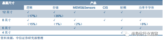
Wafer Size Corresponding Product Types
Looking at specific downstream applications, 12-inch wafers with advanced processes below 20nm have robust performance, mainly used in mobile devices and high-performance computing, including smartphone main chips, computer CPUs, GPUs, high-performance FPGAs, and ASICs. The 14nm-32nm advanced processes are applied in DRAM, NAND Flash storage chips, mid-to-low-end processor chips, image processors, digital TV set-top boxes, etc. The 12-inch 45-90nm mature processes are mainly used in areas with slightly lower performance requirements but high demands for cost and production efficiency, such as mobile basebands, WiFi, GPS, Bluetooth, NFC, ZigBee, NOR Flash chips, MCUs, etc. The 12-inch or 8-inch 90nm to 0.15μm are mainly used in MCUs, fingerprint recognition chips, image sensors, power management chips, LCD driver ICs, etc. The 8-inch 0.18μm-0.25μm mainly includes non-volatile storage such as bank cards, SIM cards, etc., while above 0.35μm is mainly for power devices such as MOSFETs and IGBTs.
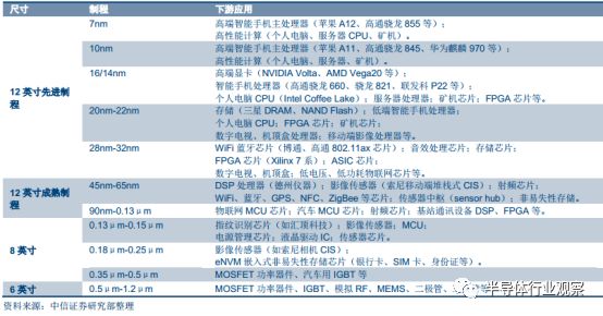
Process-Size Corresponding Downstream Application Demand Split
Compound Semiconductors: Key Materials for 5G, 3D Sensing, and Electric Vehicles
The supplier landscape for compound semiconductor wafers is dominated by Japan, the US, and Germany, forming an oligopoly.
In the substrate market, high technical barriers lead to an oligopoly in the compound semiconductor substrate market, dominated by manufacturers from Japan, the US, and Germany. Currently, GaAs substrates are occupied by four companies: Japan’s Sumitomo Electric, Germany’s Freiberg, the US’s AXT, and Japan’s Sumitomo Chemical, with these four accounting for over 90% of the market. Sumitomo Chemical acquired Hitachi Cable’s (Hitachi Metals) compound semiconductor business in 2011 and transferred it to its subsidiary Sciocs in 2016. The self-supporting GaN substrates are currently monopolized by three Japanese companies: Sumitomo Electric, Mitsubishi Chemical, and Sumitomo Chemical, accounting for over 85% of the market. The leading SiC substrate manufacturer is the US’s Cree (Wolfspeed division), with a market share of over one-third, followed by Germany’s SiCrystal, the US’s II-VI, and Dow Corning, with the four accounting for over 90%. In recent years, China has also seen the emergence of SiC substrate manufacturers with certain production capabilities, such as TianKe HeDa Blue Light.
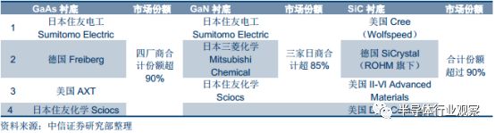
Competitiveness of Compound Semiconductor Suppliers
In the epitaxy growth market, UK-based IQE holds over 60% market share, making it the absolute leader. IQE and Taiwan’s Allnew Optoelectronics together account for 80%. The epitaxy growth mainly includes two technologies: MOCVD (Metal-Organic Chemical Vapor Deposition) and MBE (Molecular Beam Epitaxy). For example, both IQE and Allnew Optoelectronics use MOCVD, while Epistar uses MBE technology. HVPE (Hydride Vapor Phase Epitaxy) technology is mainly applied to the production of GaN substrates.
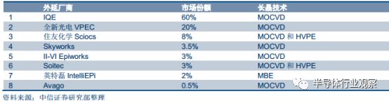
Competitiveness of Compound Semiconductor Epitaxy Manufacturers
Compound Semiconductor Wafer Demand Supplier Landscape: IDM and Foundry Giants Coexist
The compound semiconductor industry chain exhibits an oligopolistic competitive landscape. IDM manufacturers include Skyworks, Broadcom (Avago), Qorvo, Anadigics, etc. In 2016, the global compound semiconductor IDM market presented a three-player oligopoly, with Skyworks, Qorvo, and Broadcom occupying market shares of 30.7%, 28%, and 7.4%, respectively, in the GaAs field. The industry chain is showing a multi-mode integration trend, with design companies de-integrating and IDM capacity outsourcing becoming an inevitable trend.
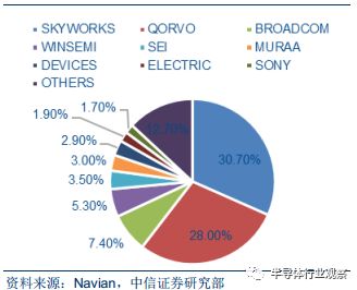
Global Gallium Arsenide Component (Including IDM) Value Distribution
The compound semiconductor wafer foundry field is dominated by Sema, accounting for 66% market share, making it the absolute leader. The second and third are AWSC and GCS, accounting for 12% and 9%, respectively. Domestic design is driving foundry, and mainland China’s compound semiconductor foundry leader is emerging. Currently, domestic PA design has seen the rise of companies such as RDA, Vanchip, Han Tianxia, and Feixiang Technology in low-end applications in consumer electronics like 2G/3G/4G/WiFi.
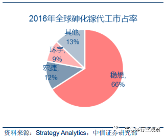
Global Gallium Arsenide Foundry Market Share
Domestic compound semiconductor design manufacturers have currently occupied low-end applications in consumer electronics for 2G/3G/4G/WiFi. Sanan Optoelectronics currently focuses on LED applications and is expected to fill the domestic gap in compound semiconductor foundry. Its fundraising production line construction is progressing smoothly, and it is expected to achieve a capacity of 4000-6000 wafers per month by the end of 2018, becoming the first large-scale GaAs/GaN compound wafer foundry enterprise in mainland China.
Compound Semiconductor Wafer Downstream Application Split: Unique Performance, Self-Contained System
The downstream specific applications of compound semiconductors can be divided into two major categories: optical devices and electronic devices. Optical devices include LED light-emitting diodes, LD laser diodes, PD optical receivers, etc. Electronic devices include PA power amplifiers, LNA low-noise amplifiers, RF switches, analog-to-digital converters, microwave integrated circuits, power semiconductor devices, Hall elements, etc. For GaAs materials, SC GaAs (single-crystal gallium arsenide) is primarily used in optical devices, while SI GaAs (semi-insulating gallium arsenide) is mainly used in electronic devices.
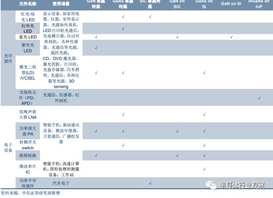
Compound Semiconductor Wafer Corresponding Downstream Applications
In optical devices, LED occupies the largest share, while LD/PD and VCSEL have significant growth potential. Cree generates about 70% of its revenue from LEDs, with the remainder coming from power, RF, and SiC wafers. SiC substrates account for 80% of the market from diodes, making SiC the most mature among all wide bandgap semiconductor substrates. Different compound semiconductor materials used for LEDs correspond to different wavelengths of light: GaAs LEDs emit red and green light, GaP emits green light, SiC emits yellow light, and GaN emits blue light. Using GaN blue LEDs to excite yellow phosphor materials can produce white light LEDs. Additionally, GaAs can produce infrared light LEDs, commonly used in remote control infrared emitters, while GaN can produce ultraviolet light LEDs. GaAs and GaN can produce red and blue laser emitters, respectively, used for reading CDs, DVDs, and Blu-ray discs.
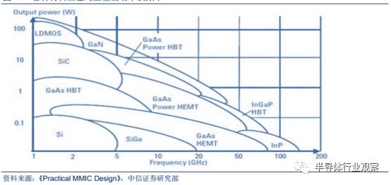
Output Power and Frequency Corresponding to Various Materials and Processes
In electronic devices, the main applications are RF and power. GaN on SiC, self-supporting GaN substrates, GaAs substrates, and GaAs on Si are primarily used in RF semiconductors (such as RF front-end PAs); while GaN on Si and SiC substrates are mainly used in power semiconductors (such as automotive electronics).
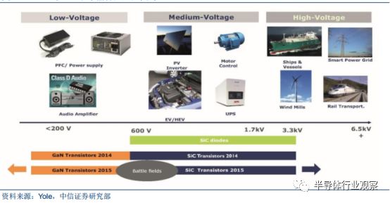
Comparison of GaN and SiC Power Device Application Ranges
Due to its high power density, GaN has unique advantages in high-power devices in base stations. Compared to silicon substrates, SiC substrates have better thermal conductivity, and currently, over 95% of GaN RF devices use SiC substrates, such as the process used by Qorvo, while silicon-based GaN devices can be manufactured on 8-inch wafers, providing a cost advantage. In the power semiconductor field, SiC substrates and GaN on Silicon only compete in a small number of areas. The GaN market is mostly in low-voltage areas, while SiC is applied in high-voltage areas. The boundary between them is around 600V.
Downstream Major Application Analysis: Examining Chip Localization from Process Materials
(1) Smartphones: IC design is catching up first, while foundry and materials still need breakthroughs.
The core chips in smartphones involve advanced processes and compound semiconductor materials, with a low localization rate. Taking Huawei smartphones, which currently use a relatively high number of domestic chips, as an example, we can roughly see the “upper limit” of domestic chips.
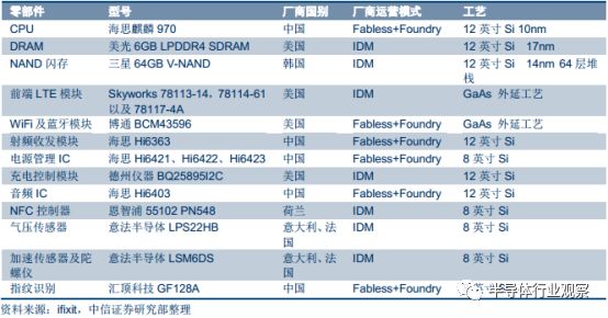
Internal Chip Correspondence Process in Huawei P20
Currently, Huawei HiSilicon can independently design CPUs, including companies like Xiaomi’s Pinecone and other fabless design companies. However, due to the use of the most advanced 12-inch processes, manufacturing primarily relies on Taiwanese companies; there are currently no domestic companies mass-producing DRAM or NAND flash; the front-end LTE modules and WiFi Bluetooth modules use GaAs materials, with production concentrated in US IDM companies like Skyworks and Qorvo and Taiwanese foundries like Sema, with no GaAs foundry manufacturers in mainland China; RF transceiver modules, PMICs, and audio ICs can be designed by HiSilicon and foundry manufactured, while charging control ICs, NFC control ICs, and sensors like pressure and gyroscopes are primarily provided by European and American IDM manufacturers. Overall, the localization rate of core chips in smartphones remains low, with some chips like DRAM, NAND, and RF modules having almost zero localization.
Taking the mainstream flagship smartphone iPhone X as an example, we can roughly see the position of mainland Chinese chip manufacturers in the global supply chain. The CPU uses Apple’s self-designed chip + TSMC advanced process foundry, DRAM and NAND come from Korean/Japanese/US IDM manufacturers; the baseband comes from Qualcomm design + TSMC advanced process foundry; the RF module uses GaAs materials, supplied by IDM manufacturers such as Skyworks and Qorvo or Broadcom + Sema foundry; analog chips, audio ICs, NFC chips, touch ICs, image sensors, etc. are all supplied by companies outside mainland China, resulting in zero share of mainland Chinese chips in Apple’s supply chain. However, most components other than chips and screens have suppliers from mainland China, with some even monopolized by mainland manufacturers. This indicates that mainland Chinese chip companies still lack competitiveness on a global scale.
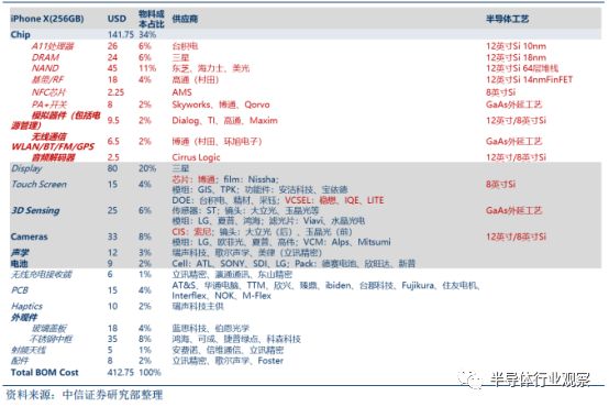
Internal Chip Correspondence Process in iPhone X
(2) Communication Base Stations: High Dependency on US Chips for High-Power RF Chips
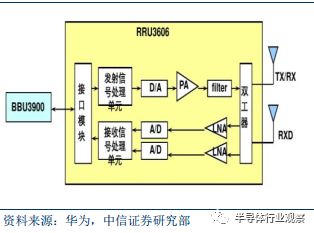
Communication base stations have a high degree of dependency on foreign chips, mainly from US chip companies. Currently, base station systems are mainly composed of a baseband processing unit (BBU) and a remote radio unit (RRU), with one BBU typically corresponding to multiple RRU devices. In comparison, the localization rate of RRU chips is lower, with a high dependency on foreign sources.
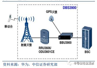
Schematic Diagram of Base Station BBU + RRU System
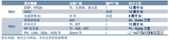
The main challenge lies in that RRU chip devices involve high-power RF scenarios, typically using GaAs or GaN materials, while mainland China lacks the corresponding industrial chain.
RRU Internal Chip with the Highest Threshold
US manufacturers monopolize high-power RF devices. Specifically, the PA, LNA, DSA, VGA chips in RRU equipment mainly use GaAs or GaN processes, supplied by companies such as Qorvo and Skyworks, where GaN devices typically use SiC substrates, i.e., GaN on SiC. RF transceivers and analog-to-digital converters use silicon-based and GaAs processes, with major manufacturers including TI, ADI, IDT, etc. All these manufacturers are US companies, leading to a very high dependency of communication base station chips on US manufacturers.
Main Chips of Base Station Communication Equipment
(3) Automotive Electronics: Industrial Technology Maturity, Some Achievements in Localization
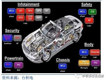
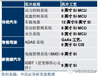
Automotive electronics primarily demand semiconductor devices such as MCUs, NOR Flash, and IGBTs. Traditional vehicles mainly have high MCU demand, including power control, safety control, engine control, chassis control, and vehicle electronics in various aspects. New energy vehicles also include electronic control units (ECUs), power control units (PCUs), vehicle control units (VCUs), hybrid vehicle controllers (HCU), battery management systems (BMS), and core components such as IGBT devices.
Internal Chips of Traditional Vehicles
In addition, NOR Flash is needed for code storage in the above-related systems, as well as in emergency braking systems, tire pressure monitoring systems, airbag systems, etc. MCUs typically use 8-inch or 12-inch 45nm~0.15μm mature processes, while NOR Flash typically uses 45nm~0.13μm mature processes, and domestic production has basically been realized.
Internal Chips of Vehicles
Semiconductor devices used in intelligent driving include high-performance computing chips and ADAS systems. High-performance computing chips currently use 12-inch advanced processes, while the millimeter-wave radar in ADAS systems involves GaAs materials, which cannot be mass-produced domestically.
(4) AI and Mining Machine Chips: New Growth Drivers, Domestic Design Manufacturers Achieve Breakthroughs
AI chips and mining machine chips belong to high-performance computing, which requires advanced processes. In AI and blockchain scenarios, traditional CPU computing power is insufficient, and new architecture chips are becoming a development trend. Currently, there are mainly paths for GPU, FPGA, ASIC (TPU, NPU, etc.) chips that continue the traditional architecture, and paths that completely subvert traditional computing architecture by adopting structures that simulate human brain neurons to enhance computing power. In the cloud domain, the GPU ecosystem is leading, while specialization in terminal scenarios is the future trend.
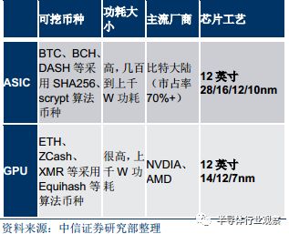
Overview of Main Mining Machine Chips
According to the technology roadmap published by NVIDIA and AMD, GPUs will enter 12nm/7nm processes in 2018. Currently, AI and mining-related FPGA and ASIC chips are also using advanced processes of 10-28nm. Domestic manufacturers such as Cambricon, Deep Insight Technology, Horizon, and Bitmain have emerged as excellent IC design manufacturers achieving breakthroughs, while manufacturing mainly relies on advanced process foundries like TSMC.
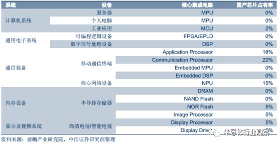
Current Domestic IC Market Share
According to IC Insight data, in 2015, China’s integrated circuit companies had only 3% of the global market share, while the US, Korea, and Japan had 54%, 20%, and 8%, respectively. In fact, even the US, Korea, and Japan cannot achieve 100% self-sufficiency in the semiconductor industry chain. For example, in the core equipment for advanced process manufacturing, photolithography machines still rely on the Dutch company ASML. More participation in global division of labor and gradually increasing the localization rate is a feasible development path for the semiconductor industry.
The domestic chip demand in the terminal market is fully equipped, and the supply side is expected to tilt towards mainland China. (1) Demand side: The downstream terminal application market is fully equipped, with gradually maturing scale conditions. As global terminal product capacity shifts to China, China has become the global manufacturing base for terminal products, with 2017 figures showing that China’s automotive and smartphone shipments accounted for 29.8% and 33.6% of the global total, respectively. Chip demand comprehensively covers the silicon-based and compound semiconductor markets, indicating a huge chip market space. (2) Supply side: Currently, there are very few IC design, wafer foundry, and storage manufacturers in mainland China that rank high in terms of output value. The technological level has not yet reached a leading level, and mid-to-high-end chip manufacturing and compound semiconductor chips are heavily reliant on imports. As terminal demand gradually shifts to mainland China along with industries such as smartphones in recent years, this demand shift may drive manufacturing transfer, and the downstream chip supply side is beginning to shift to the mainland.
Domestic Policies Accelerating the Development of the Semiconductor Industry. In recent years, China has issued a series of supportive policies for the integrated circuit industry, continuously optimizing the financing, tax, and subsidy policy environment. Especially the “National Integrated Circuit Industry Development Promotion Outline” issued in June 2014, which set the tone that “design leads, manufacturing is fundamental, and equipment and materials are supportive”, aiming to promote the development of China’s integrated circuit industry with growth cycles set for 2015, 2020, and 2030: By 2015, the integrated circuit industry sales revenue should exceed 350 billion yuan; by 2020, the integrated circuit industry sales revenue should achieve an average annual growth rate of over 20%; by 2030, the main links of the integrated circuit industry chain should reach internationally advanced levels, and a batch of enterprises should enter the international first tier, achieving leapfrog development.
Transferred from: “Semiconductor Industry Observation”