
Table of Contents
1. Frequency Characteristics and Application Scenarios
1. Low Frequency Band (kHz): Fundamental Support for Large Area Processes
2. Mid-High Frequency Band (MHz): Main Frequencies for Etching and Deposition
3. High Frequency Band (60MHz and above): Core Frequencies for Advanced Processes
4. Impact of Wafer Size on Frequency Selection
5. Comparison of Common Frequency Characteristics and Application Scenarios
2. Factors Influencing Selection Decisions
1. Frequency Selection Driven by Process Requirements
2. Physical Constraints and Equipment Compatibility
3. Core Technical Parameter Requirements
4. Regulatory and Cost Constraints
5. Construction of Selection Decision Trees
1. Frequency Characteristics and Application Scenarios
The characteristic parameters of RF frequency (such as penetration depth and plasma density) are core factors determining their application scenarios. In precision processes such as semiconductor manufacturing, frequency selection must match the process goals (such as deposition uniformity and etching accuracy) and wafer size depth, forming an application gradient from low frequency to high frequency.
1. Low Frequency Band (kHz): Fundamental Support for Large Area Processes
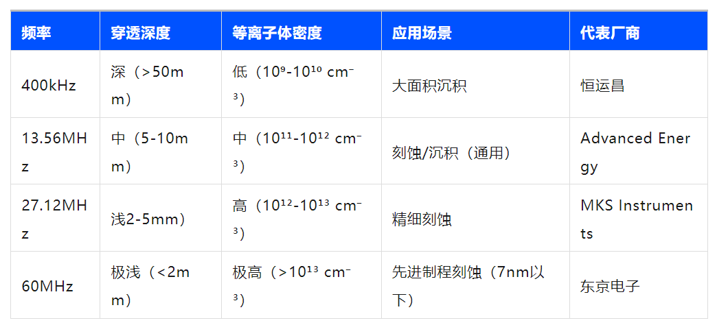
400kHz is a typical low frequency representative, characterized by deep penetration depth (>50mm) and low plasma density (10⁹-10¹⁰ cm⁻³). This characteristic makes it outstanding in large area thin film deposition: when RF energy is coupled to the plasma chamber at a frequency of 400kHz, electromagnetic waves can penetrate thicker gas layers, ensuring that the plasma is evenly distributed on the surface of 8-inch or 12-inch wafers, especially suitable for large area deposition processes of insulating films such as silicon oxide and silicon nitride.
2MHz frequency plays a supporting role in etching processes. Its penetration depth is moderate (10-20mm), and plasma density is slightly higher than that of 400kHz (10¹⁰-10¹¹ cm⁻³), mainly used to control ion bombardment energy.
2. Mid-High Frequency Band (MHz): Main Frequencies for Etching and Deposition
13.56MHz is the most widely used RF frequency in semiconductor manufacturing, characterized by moderate penetration depth (5-10mm) and moderate plasma density (10¹¹-10¹² cm⁻³), suitable for both etching and deposition processes.
In plasma etching, the 13.56MHz RF power supply can stably generate plasma with moderate density, achieving precise etching of different materials such as silicon and metals by adjusting power, with a market share exceeding 50%.
27.12MHz and 40.68MHz frequencies, with higher plasma densities (10¹²-10¹³ cm⁻³) and shallower penetration depths (2-5mm), have become key choices for fine etching.
In the etching of contact holes in logic chips, the 27.12MHz RF power supply can generate high-density plasma, ensuring protection of the sidewalls of high aspect ratio structures; while 40.68MHz performs excellently in the step etching of 3D NAND, with MKS Instruments’ products in this frequency range already supporting the mass production process of 176-layer flash memory.
3. High Frequency Band (60MHz and above): Core Frequencies for Advanced Processes
60MHz frequency, with extremely shallow penetration depth (<2mm) and extremely high plasma density (>10¹³ cm⁻³), has become the core for advanced processes below 7nm. In the etching of FinFET and GAA architectures, the 60MHz RF power supply can generate highly ionized plasma, achieving precise control over nanoscale feature sizes.
For example, Tokyo Electron’s advanced etching machines use a dual-frequency combination of 60MHz and 2MHz, controlling plasma density with high frequency and adjusting ion energy with low frequency, meeting the stringent requirements for etching accuracy (CD uniformity <1nm) in 3nm processes.
4. Impact of Wafer Size on Frequency Selection
Large size wafers of 300mm and above pose higher requirements for frequency combinations. Since a single frequency is difficult to meet uniformity at both the edge and center, dual-frequency or multi-frequency coupling technology has become mainstream.
For example, the third-generation dual-frequency capacitive coupled plasma source (CCP) adopts a strategy of “low frequency to control ion energy + high frequency to control plasma density,” where the high frequency is usually 4-10 times that of the low frequency.
North Huachuang’s ICP etching machine uses a combination of 2MHz and 27.12MHz to achieve etching rate uniformity <3% on 300mm wafers;
Applied Materials’ Endura deposition system solves the film stress distribution problem on large size wafers through a dual-frequency power supply of 13.56MHz and 60MHz.
Core Logic of Frequency Selection:
Low frequency (400kHz/2MHz) dominates large area uniformity processes due to its deep penetration advantage.
Mid-high frequency (13.56MHz/27.12MHz) balances density and control precision, becoming a general choice.
High frequency (60MHz) meets advanced process requirements through extremely high plasma density.
300mm wafers require dual-frequency combinations to achieve “energy-density” collaborative control, a logic that runs through the entire process of semiconductor etching and deposition.
5. Comparison of Common Frequency Characteristics and Application Scenarios
2. Factors Influencing Selection Decisions
The selection of RF systems needs to construct a systematic decision-making framework of “demand → constraints → selection,” integrating process objectives, equipment characteristics, technical parameters, and regulatory requirements to form an operable selection path. The following analysis unfolds from core dimensions:
1. Frequency Selection Driven by Process Requirements
Different semiconductor manufacturing processes have significantly differentiated demands for RF frequencies, requiring priority matching with process objectives:
Etching Process: To enhance plasma density and etching rate, high frequencies above 27.12MHz are preferred, such as 60MHz commonly used for advanced logic chip etching; while metal etching often uses 400 kHz low frequency to control ion energy and reduce damage to underlying materials..Deposition Process: Focused on film uniformity, mainstream choice is 13.56MHz mid-frequency, balancing plasma stability and energy control..Wafer Size Adaptation: For large size wafers of 300mm and above, dual-frequency combinations are recommended (such as 2MHz+27 MHz), using low frequency to control ion energy and high frequency to enhance uniformity, achieving a balance between efficiency and process indicators.24.
Typical Correspondence Between Frequency and Process is shown in the table below:
| Application Scenario | Recommended Frequency | Core Objective |
|---|---|---|
| Metal Etching | 400 kHz | Reduce ion energy, protect the substrate |
| Dielectric Etching | 27 MHz | Enhance etching rate and anisotropy |
| Thin Film Deposition | 13.56 MHz | Optimize film uniformity and density |
| 300 mm Wafer Process | 2 MHz+27 MHz Dual Frequency | Balance global uniformity and local precision |
2. Physical Constraints and Equipment Compatibility
Frequency selection must overcome the dual constraints of physical limitations and equipment parameters to ensure stable system operation:
Avoiding Standing Wave Effects: When the electrode size exceeds 1/10 of the wavelength at the operating frequency, standing waves can easily occur, leading to deterioration of process uniformity. For example, the wavelength of the second harmonic (120 MHz) of a 60 MHz power source is 2.5 m, and the electrode diameter must be controlled within 250 mm to avoid standing waves..
Impedance Matching: Inductive impedance increases with frequency (XL=2πfL), while capacitive impedance decreases (XC=1/(2πfC)), requiring matching of RF matcher Q value and transmission line length (optimal is λ/4).16.Plasma Property Control: When the pulse repetition frequency is increased from 10 kHz to 50 kHz, plasma density can increase by 1.8 times, and the standard deviation of ion bombardment angle distribution decreases by 42%; using a frequency sweep mode (e.g., 80±20 kHz) can suppress abnormal discharges caused by resonance.26.
3. Core Technical Parameter Requirements
Frequency selection must quantitatively assess key parameters to ensure signal quality and process consistency:
Frequency Accuracy and Stability: For example, the ACE 5400 signal generator has a frequency accuracy of 0.025% or 2.0 kHz, avoiding signal drift that affects process repeatability..Amplitude Characteristics: Including amplitude range (e.g., +30 to +50 dBmv), accuracy (±1.0 dB), and step (1 dB), directly affecting plasma energy control precision..Frequency Spectrum Purity: Must be ≥-55 dBc to reduce spurious interference, suitable for sensitive quantum dot etching scenarios..
For components such as RF switches and filters, the following must also be considered:
Switch Parameters: Frequency range (e.g., 1-5 GHz, 3-10 GHz), power handling capability (linearity, ACLR, IP3, EVM), switching speed, and impedance standards (50Ω is primary, some 75Ω)..
Filter Selection: Battery-powered devices prioritize low IL (insertion loss) types for energy saving, while power-connected devices require high attenuation performance; custom matching chip group filters or standard off-the-shelf components can be selected..
4. Regulatory and Cost Constraints
Frequency Band Compliance: ISM band must pay attention to national licensing differences, such as Europe ETSI and US FCC opening new frequency bands, and Australia clearly defining sub-band uses for the 2 GHz band; power transmission must not exceed 100 mW equivalent isotropic radiated power (EIRP)..
Cost Gradient: The average price of RF generators increases with frequency, with the cost of the 400kHz low frequency band significantly lower than that of the 60 MHz high frequency band, requiring a balance between technical needs and budget..
5. Construction of Selection Decision Trees
Based on the above analysis, RF system selection can follow the following path:
Clarify process objectives: Etching (high frequency)/deposition (mid frequency), material type (metal/dielectric), wafer size (300 mm requires dual frequency);
Assess physical constraints: Relationship between electrode size and wavelength (avoid standing waves), impedance matching requirements, plasma parameter control targets;Quantify parameter indicators: Frequency accuracy, amplitude characteristics, frequency spectrum purity, matching switch/filter parameters;Compliance and cost balance: Confirm frequency band licensing, combine high-frequency technology added value with budget to select the optimal solution.
Key Decision Nodes:300 mm wafer processes prioritize the 2 MHz+27 MHz dual frequency combination, metal etching limits to 400 kHz low frequency, and high frequency bands require simultaneous assessment of standing wave effects and cost gradients.
Welcome to join the semiconductor equipment and process exchange group~Please add the editor, and note your company+Name+Position.
 Disclaimer: The content of this article comes from the public account (Semiconductor Pony), and is only used for organizing and promoting semiconductor industry knowledge, with no commercial purpose. Thanks to the original author. If there is any offense or infringement, please contact for deletion. Thank you~