The contact resistance of transistors at advanced nodes in integrated circuits has sharply increased with the continuous miniaturization of devices, becoming a critical bottleneck at the physical limits of Moore’s Law. Driven by Moore’s Law, device sizes continue to shrink, and the transistor source-drain contact resistance, which is inversely proportional to the contact area, has sharply increased. At the 5nm process node, the contact resistance accounts for 38% of the total transistor resistance, exceeding 50% at the 3nm process node, and is expected to be even higher at the 2nm node. Contact resistance has become a key bottleneck limiting the performance improvement of devices at advanced process nodes.
According to international roadmap requirements, the contact resistivity at process nodes below 2nm must be reduced to 10⁻⁹ Ω·cm². The core challenge lies in the strong Fermi Level Pinning (FLP) effect at the metal-semiconductor contact interface, which causes the Fermi level of the metal to be pinned near the top of the semiconductor valence band, resulting in a Schottky barrier height that does not decrease significantly with changes in the metal work function, thus leading to a large intrinsic contact resistance. Among all semiconductors, germanium exhibits the strongest Fermi Level Pinning effect, with a pinning factor S = 0.02, close to the Bardeen limit S = 0. Traditional views suggest that metal electronic states within the semiconductor bandgap penetrate into the semiconductor, forming Metal-Induced Gap States (MIGS), which lead to the Fermi Level Pinning effect. Since the density of MIGS is inversely proportional to the semiconductor bandgap width, a narrower bandgap results in a higher MIGS density and a stronger pinning effect, thus the Fermi Level Pinning effect is considered an intrinsic property of semiconductor materials.
Recently, a team led by Academician Li Shushen and Researcher Luo Junwei from the National Key Laboratory of Semiconductor Chip Physics and Technology at the Chinese Academy of Sciences used first-principles calculations to reveal a new physical mechanism for the Fermi Level Pinning effect at the metal-semiconductor contact interface. The research team found that surface states induced by dangling bonds in semiconductors play a crucial role in the Fermi Level Pinning effect, with an impact comparable to that of Metal-Induced Gap States (MIGS). The key to germanium’s strong Fermi Level Pinning effect lies in the tendency of germanium and silicon to form different bonding configurations at the interface. The dangling bond states at the semiconductor interface form new bonding and antibonding states after reconstruction, with electrons on the dangling bonds fully occupying the new bonding states, thereby lowering the system energy. The energy gained from reconstruction is inversely proportional to the square of the bond length, making silicon thermodynamically and kinetically inclined to maintain a stable spontaneous in-plane bonding configuration (Figure 1). The in-plane bonding forms a self-passivation effect, effectively passivating the dangling bonds and reducing the interface state density, resulting in a weaker Fermi Level Pinning effect for silicon (pinning factor S = 0.16). In contrast, the atomic bond length of germanium is 4.3% larger than that of silicon, and the energy gained from reconstruction is minimal, leading germanium to tend to maintain a non-reconstructed interface, retaining more dangling bonds and interface states after bonding with the metal, resulting in a very strong Fermi Level Pinning effect (S = 0.02). From germanium to silicon to diamond, the interatomic distance decreases sequentially, enhancing the self-passivation effect of the interface dangling bonds, leading to a decrease in the density of surface states induced by dangling bonds and a corresponding reduction in the Fermi Level Pinning effect.
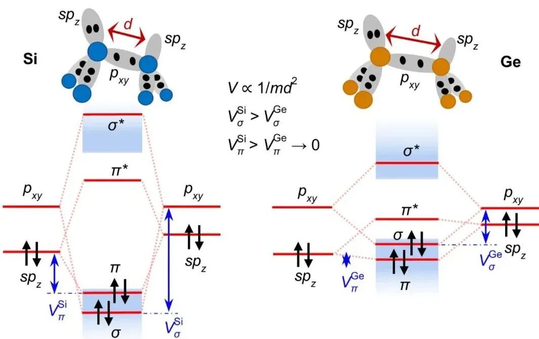
Figure 1: The breaking of bonds at the semiconductor interface generates a high density of surface states, leading to a strong Fermi Level Pinning effect. The self-passivation effect of in-plane bonding effectively passivates dangling bonds, reducing the Fermi Level Pinning effect in silicon.
The research team further extended this mechanism to a broader range of semiconductor systems, discovering that as the ionic character of the semiconductor increases, the dangling bond-induced surface states deep within the bandgap gradually disappear, significantly weakening the Fermi Level Pinning (Figure 2). The established unified physical framework of “interface bonding – dangling bond density – pinning strength” provides a reliable theoretical basis for evaluating and predicting the contact characteristics of different material systems.
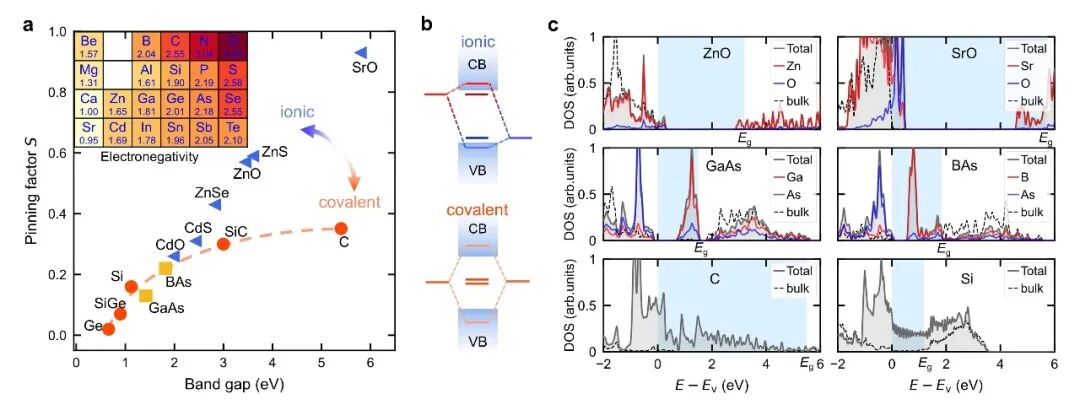
Figure 2: The intrinsic relationship between semiconductor ionic character, dangling bond-induced surface states, and Fermi Level Pinning strength. As ionic character increases, the density of dangling bond-induced surface states deep within the bandgap significantly decreases, leading to a corresponding reduction in pinning strength; conversely, semiconductors with stronger covalency exhibit higher densities of dangling bond-induced surface states deep within the bandgap, resulting in stronger pinning even with similar bandgap widths.
The research team theoretically demonstrated that the passivation effect of dangling bonds can be significantly enhanced by introducing external non-metal atoms, thereby greatly reducing the density of dangling bond-induced surface states. The study showed that using hydrogen atoms can perfectly passivate the dangling bonds at the silicon and germanium interfaces, eliminating all dangling bond-induced surface states, thereby significantly weakening the Fermi Level Pinning effect, raising the pinning factors of silicon and germanium from 0.16 and 0.02 to 0.5 and 0.45, respectively (Figure 3). This allows various metals to reduce the Schottky barrier at the silicon and germanium interfaces to nearly ideal zero values, providing a new approach to reducing contact resistivity to the international roadmap requirement of 10⁻⁹ Ω·cm² for process nodes below 2nm.
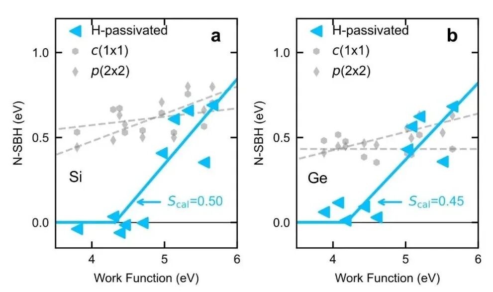
Figure 3: Using hydrogen atoms can perfectly passivate the dangling bonds at the silicon and germanium interfaces, eliminating all dangling bond-induced surface states, thereby significantly weakening the Fermi Level Pinning effect, raising the pinning factors of silicon and germanium from 0.16 and 0.02 to 0.5 and 0.45, respectively.
This work breaks through the limitations of traditional Metal-Induced Gap States (MIGS) theory, proposing a new approach to suppress FLP by controlling the bonding configurations of interface atoms, providing new insights for overcoming the contact resistance bottleneck in future advanced technology nodes.
This purely theoretical research result, titled “Self-passivation reduces the Fermi level pinning in the metal-semiconductor contacts,” was published on November 27 in Nature Communications. Researcher Luo Junwei, director of the National Key Laboratory of Semiconductor Chip Physics and Technology, is the corresponding author, and PhD student Xiang Ziying is the first author. This research was supported by the National Natural Science Foundation of China (Project No. 12525402) and the Stable Support Youth Team of the Chinese Academy of Sciences (Project No. YSBR-026).
Article link: https://doi.org/10.1038/s41467-025-65695-y
END
The reproduced content only represents the author’s views
It does not represent the position of the Semiconductor Research Institute of the Chinese Academy of Sciences
Editor: Yi Er
Responsible Editor: Catnip
Submission Email: [email protected]
Previous Recommendations
1. Understanding the Differences Between DDR4 and DDR5 DRAM
2. What is Local Reflow in TCB Technology?
3. How to Significantly Improve TCB Process Capacity?
4. Introduction to Post-CMP Cleaning
5. Chip Manufacturing: Controlling Electric Fields with Dielectric Materials
6. How to Understand PDK in Wafer Manufacturing?