In semiconductor manufacturing, have you often heard about “CMP” but are unclear about what it actually does? How do we solve the uneven surface of chips? Why is it indispensable for multilayer wiring? This comprehensive guide on CMP (Chemical Mechanical Polishing) breaks down the principles, applications, materials, and equipment workflow clearly. Whether you are a newcomer to the industry or an experienced professional, save this for direct use and easily understand the core technology of chip “smoothing and polishing”!
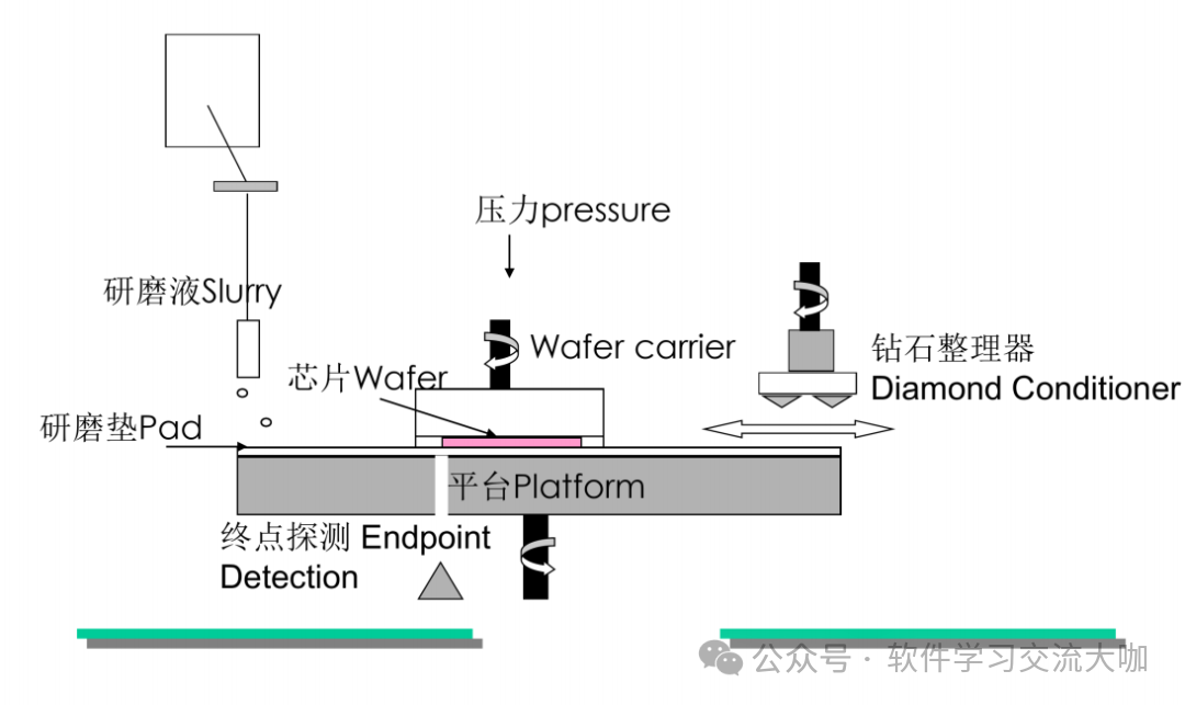
1. First, understand: What is CMP? Why is it a “must-have” in chip manufacturing?
CMP (Chemical Mechanical Polishing) is simply put asa combination of “chemical etching + mechanical grinding” to polish the wafer surface to a smooth finish, equivalent to giving the chip a “high-precision polish”.
Why is it indispensable? Without CMP, the chip surface is “uneven”:
- Multilayer metal wiring can cause short circuits and signal transmission issues due to unevenness;
- During lithography, uneven surfaces can lead to pattern distortion, drastically reducing yield;
- It is impossible to achieve high-density integration (such as stacking transistors in 5nm chips).
However, CMP can achieve “comprehensive flattening”, which is a key technology for the semiconductor industry to transition from micron-level processes to nanometer-level processes—without it, there would be no high-end chips today!
2. Core content: The 4 main application scenarios of CMP (collectible table)
CMP runs through the “front end (FEOL) + back end (BEOL)” of chip manufacturing, with different processes corresponding to different polishing targets, directly matching:
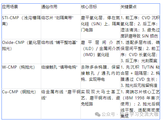
Key point: In addition to these 4 types, there are also Poly-CMP (polysilicon polishing), RGPO-CMP, etc., all focusing on “precise polishing + damage-free flattening”!
3. CMP’s “three treasures”: material selection + influencing factors
The polishing effect of CMP relies entirely on 3 core materials; choosing and using them correctly is essential to ensure yield:
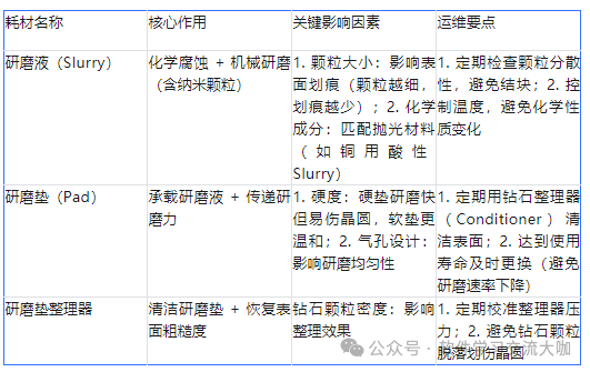
Warning: The lifespan of materials directly affects the polishing effect! For example, if the polishing pad is used for too long, the polishing rate will decrease, and the uniformity (Nu%) will exceed the standard, necessitating regular machine monitoring (ROUTINE MONITOR)~
4. Equipment operation: 6-step workflow of the Mirra-Mesa machine (copy this for your work)
Taking the mainstream Mirra-Mesa machine as an example, the complete CMP process is crystal clear, and every step must be correct:
- Take wafer: The FABS robotic arm takes the unprocessed wafer from the cassette and sends it to the temporary holding area;
- Load: The machine’s robotic arm transfers the wafer to the LOADCUP (loading/unloading platform), secured by the HEAD (wafer carrier head);
- Polish: The CROSS rotation drives the HEAD, polishing in the order of PLATEN1→2→3 (pressure + polishing liquid + polishing pad work together);
- Unload: After polishing, the wafer returns to the LOADCUP for unloading;
- Clean: The wafer is sent to the MESA cleaning area, undergoing 4 cleaning steps: ammonia + ultrasonic cleaning → ammonia scrubbing → hydrofluoric acid scrubbing → spin drying;
- Return to cassette: The cleaned wafer is sent back to the original cassette, completing the entire process.
Key point: Never skip the cleaning step! The polished wafer surface has residues of polishing liquid and particles; failure to clean will lead to defects in subsequent processes~
5. History of CMP development + key milestones (quick overview)
- 1983: IBM invented the CMP process, ushering in a new era of chip flattening;
- 1986: Oxide CMP began trial implementation;
- 1992: CMP was included in the SIA technology roadmap, becoming a standard process;
- 1994: Taiwanese semiconductor manufacturers first used CMP for mass production;
- 1998: IBM first used copper process CMP (Cu-CMP), promoting the development of high-end chips.
6. Operational pitfalls: 3 key points (reduce 90% of failures)
- Regularly monitor parameters: Focus on polishing rate (Removal Rate) and uniformity (Nu%), and adjust materials or machine parameters promptly if they exceed control limits;
- Pay attention to endpoint detection: Use optical or friction current signals to determine the polishing endpoint, avoiding over-polishing (e.g., STI-CMP wearing through the SiN layer) or under-polishing;
- Maintain a clean environment: Polishing liquids and pads are prone to contamination, requiring operation in a Class 100 cleanroom to avoid particle impurities causing scratches on the wafer.
Interaction time
Have you encountered surface scratches, poor polishing uniformity, or inaccurate material lifespan control in the CMP process? Share your practical challenges in the comments!
#Semiconductor CMP #Chemical Mechanical Polishing #Semiconductor Manufacturing #Chip Flattening #Wafer Polishing #Semiconductor Process #Chip Manufacturing Insights