In high-speed signal generation applications, bandwidth and resolution are critical requirements. New signal generation applications utilize high-speed digital-to-analog converters (DACs) to produce various types of waveforms, including single tones with true hundreds of megahertz bandwidth and complex multi-channel waveforms. These applications require high-speed DACs to be fast enough to generate these waveforms without sacrificing analog performance. In many signal generation applications, phase noise can limit the number of channels and the possible channel spacing. Traditionally, phase noise is caused by the clock signal driving the DAC’s clock input; however, any phase noise added by the DAC will appear in the output spectrum and limit the signals that can be generated. For any general signal generation application, the ideal DAC speed should be as fast as possible, with low noise, high linearity, and very low additive phase noise. If any of these performance specifications are lacking, the generated waveforms will not meet the application requirements.
Bandwidth
In any signal generation application, the most important design criterion is bandwidth. The first question any designer will ask is: how much bandwidth is needed to generate the desired signal? For specific signal protocols or applications, designers may require a certain amount of bandwidth. Regardless of how large the bandwidth a designer wants to achieve, the DAC speed must be at least twice the desired bandwidth. The relationship between bandwidth and sampling rate  is defined by the Nyquist theorem, which describes the behavior of signals in a sampling system.
Although signals can be generated with bandwidths ranging from DC to  , doing so is often impractical because mirror frequency signals of the generated signal will appear in the output spectrum. Mirror frequency signals will appear at
 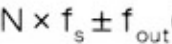 (where
  is the frequency of the generated signal), and in practice, a reconstruction filter is needed to attenuate any mirror frequency signals that may appear in the output spectrum. Even if the bandwidth of the generated signal does not extend to
  , but is close to it, mirror frequency signals will still be difficult to avoid. Reconstruction filters are implemented in the analog domain using real components, which are non-ideal and lead to non-ideal passbands with ripple and insertion loss, unlike digital filters. Generally, the higher the order of these filters, the greater the ripple and insertion loss, making ideal filters more difficult to design. The closer the signal bandwidth is to
  , the higher the filter order must be to attenuate the mirror frequency signals generated during sampling. The higher the filter order, the more components are required, leading to greater insertion loss and passband ripple.
Using a DAC with a higher sampling rate increases the available bandwidth, which reduces the requirements for the filter, allowing the filter to use fewer components, thereby simplifying the design and yielding better results. The LTC2000 is a high-performance, 16-bit, 2.5Gbps high-speed DAC with a 2.5Gbps sampling rate, allowing for  frequencies of 1.25GHz. Therefore, for an 800MHz signal bandwidth, there will be a mirror frequency signal at 1.7GHz. There is a 900MHz guard band between the desired band and the mirror frequency signal frequency, allowing the mirror frequency signal to be easily filtered out with a simple low-pass filter. Mirror frequency signals generated by DACs with lower sampling rates are closer to the desired frequency, thus requiring stricter and more complex filters.
To generate signals with bandwidth extending to  , there is another issue: any DAC has SINC (sin(x)/x) roll-off, which causes the generated signal to attenuate as frequency increases. This roll-off has a zero at the sampling frequency
  , making it impossible to generate a signal that accurately appears at the sampling frequency. The generated signal is merely a DC voltage; for practical applications, about 60% of the Nyquist region
  does not have significant SINC attenuation and can be utilized. If 0dB is the signal level at DC, then at 60% of the Nyquist frequency, the signal level will drop by 6dB. This roll-off is often compensated in the digital domain to correct the generated signal’s roll-off. This allows the DAC to produce waveforms with a constant amplitude that varies with frequency. If a higher-speed DAC is used, the SINC function’s roll-off will diminish as the DAC output frequency increases.
Phase Noise
Another important factor to consider in signal generation applications is the output phase noise. The phase noise present in the output signal limits the spacing between signals and may restrict the modulation order that can be achieved. During signal generation, the greater the phase noise, the lower the SNR of the generated signal, and the higher the bit error rate. Jitter can be used to measure the zero-crossing accuracy of the signal in the time domain; a perfect signal would cross zero at the same time in each cycle. In reality, these zero-crossing points will have some dispersion in time. If this dispersion translates to the frequency domain, phase noise can be seen as spectral leakage around the fundamental frequency. If several tones are close in phase, a common SNR may degrade due to the spectral leakage of adjacent tones, which can worsen the signal’s bit error rate and reduce the accuracy of the generated signal. By reducing the phase noise introduced in the generated signal, this loss of signal integrity can be avoided.
The simplest way to avoid introducing phase noise into the signal generation system is to use a clock with very low phase noise to drive it. A clock with low phase noise will pass on lower phase noise to the generated signal. It is also important that the attenuation of the phase noise in the generated signal is proportional to the ratio of the generated signal frequency to the clock sampling rate. This proportional relationship means that generating a low-frequency signal with the same clock will produce less phase noise on the output signal compared to generating a high-frequency signal with a high sampling frequency clock. If the generated spectrum is wide, then at the high end of the spectrum, the generated signal will have greater phase noise relative to the lower frequency end.
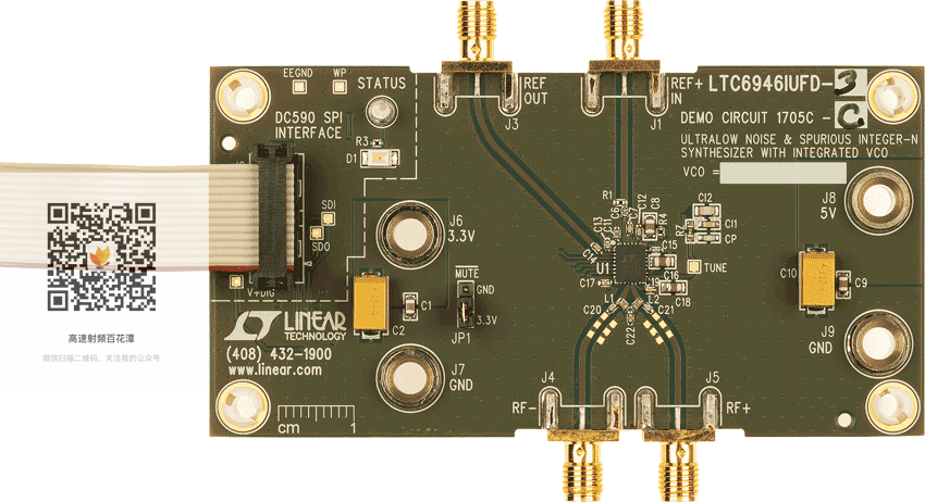
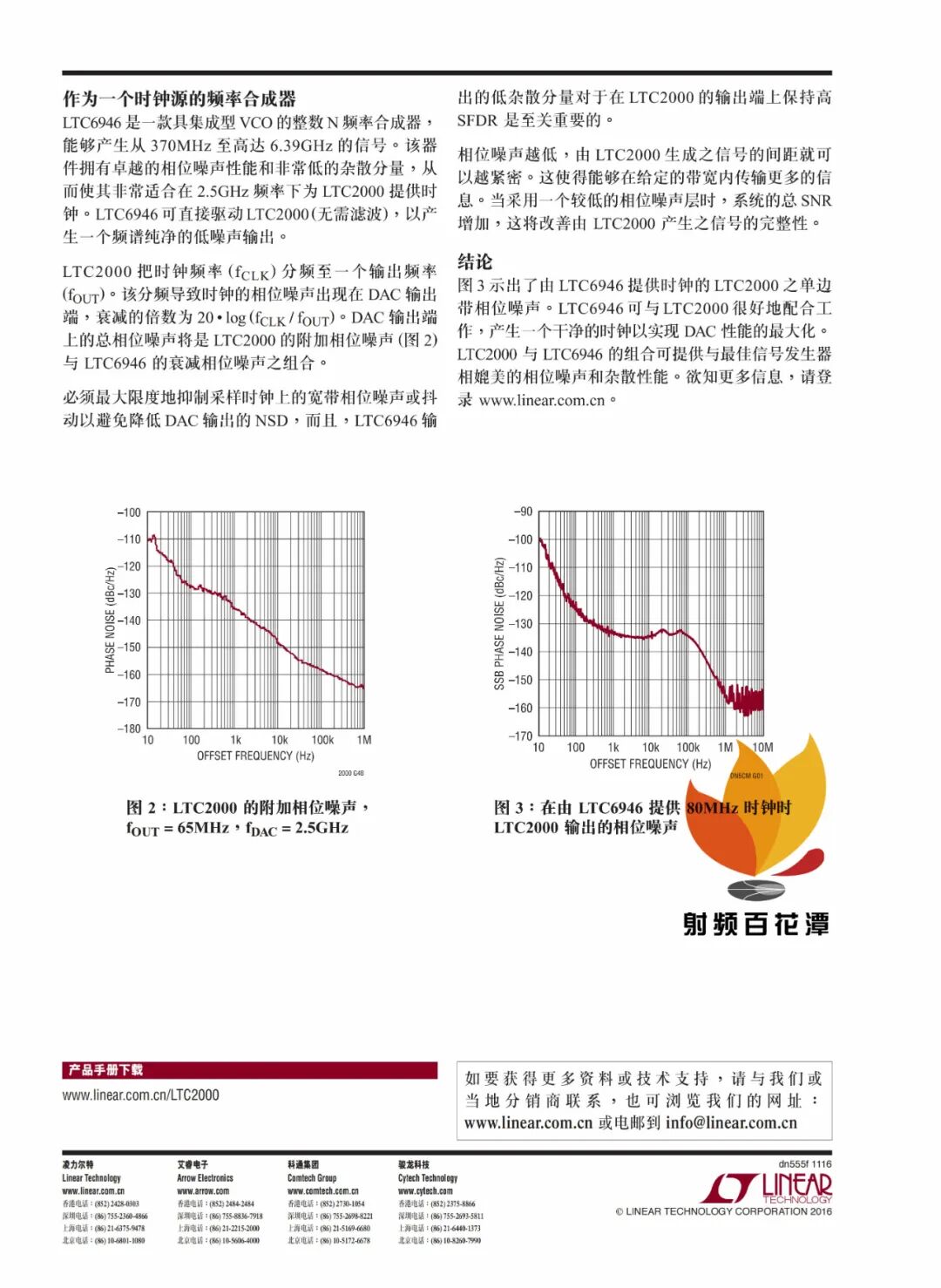
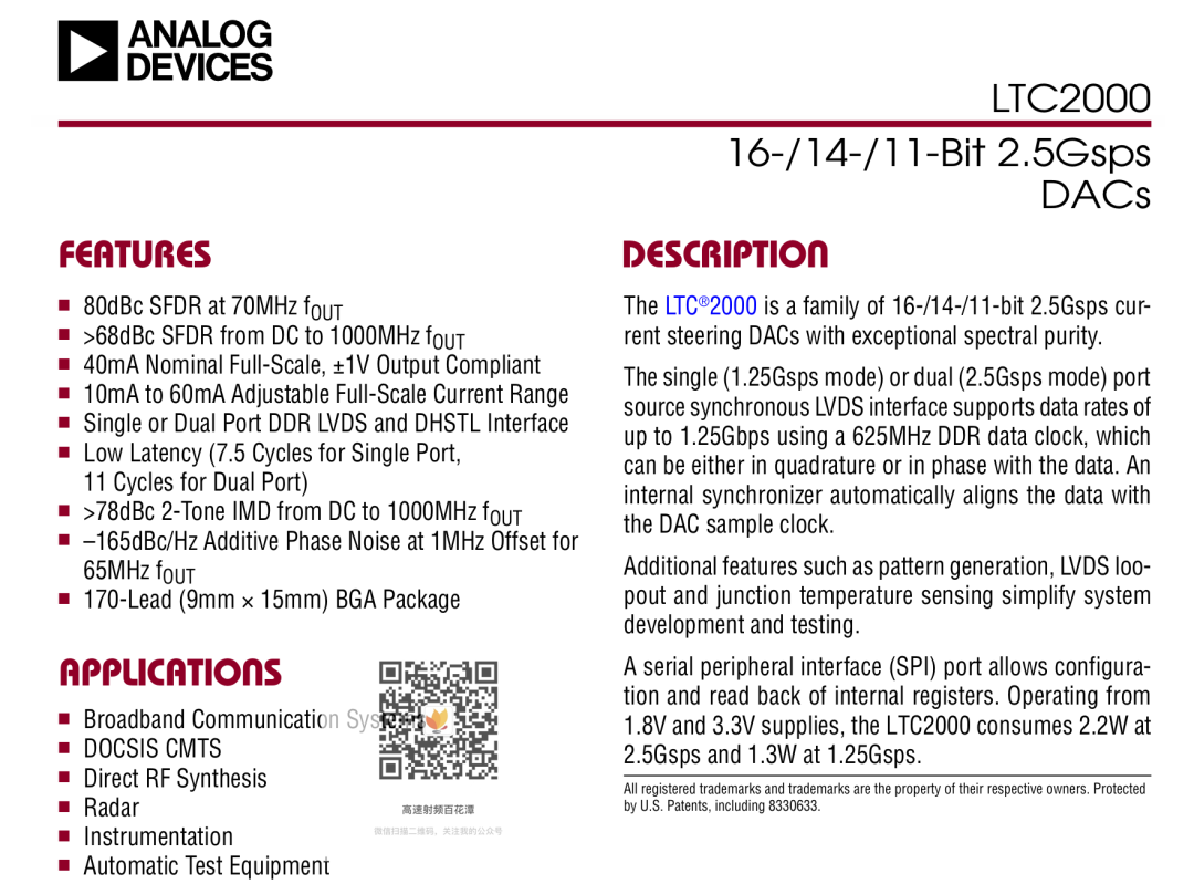
The LTC6946 is a frequency synthesizer that can generate signals from 370MHz to 5.7GHz without an external VCO. This device features excellent phase noise performance and very low parasitic components, making it suitable as a clock source for signal generation applications. When driving the LTC2000 high-speed DAC with the LTC6946, the generated phase noise is low enough to meet the requirements of most demanding signal generation applications. The LTC6946 includes an internal VCO, allowing a trade-off between convenience and phase noise. If the LTC6945 and an external VCO are used, even lower phase noise can be achieved. For the LTC6945 and LTC6946 frequency synthesizers, the dominant phase noise is from the VCO. When generating a 65MHz output tone, the LTC2000 has an additional noise of -165dBc/rHz at a 1MHz offset, ensuring that the clock phase noise is dominant compared to the LTC2000’s own additive phase noise. To avoid other noise degrading the output signal, proper layout techniques should be employed in the analog output circuit.
Proper RF Layout
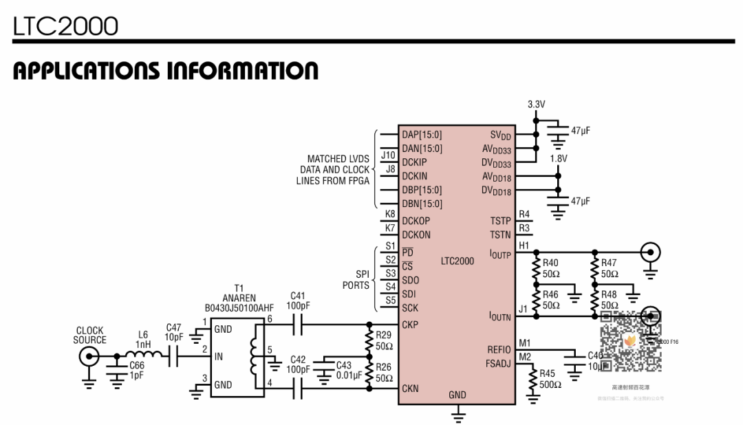
When designing printed circuit boards, if proper design and layout rules are not followed, the benefits of using high-performance DACs and clock sources will be significantly diminished. Without appropriate symmetry, bypassing, and barriers, the generated analog output waveform may exhibit errors. This can introduce noise and other parasitic components. Figure 1 shows a typical schematic of the LTC2000, which has a noise spectral density better than 158dBm/rHz up to 500MHz, helping to maintain a high signal-to-noise ratio across a wide range of signal frequencies. The device’s spurious-free dynamic range (SFDR) is better than 74dB up to 500MHz, and for output frequencies up to 1GHz, the SFDR is better than 68dB. To maximize the performance of the LTC2000, proper layout is essential. The DAC’s output should be treated as a differential pair and transmitted along symmetrical paths whenever possible. Any asymmetry in the output network can lead to voltage differences between the differential signals. This voltage difference will cause common-mode interference, resulting in unwanted distortion and noise in the output spectrum. By ensuring symmetry in the transmission lines of each output, this interference can be avoided.
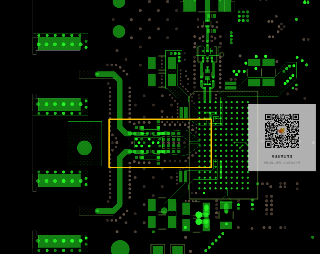
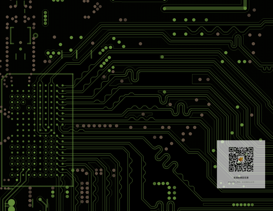
Analog outputs can be protected from interference signals through vias and good layout. The signal generation DAC has three ports, presenting layout challenges: clock input, analog output, and data input. If the data input traces run close to the output or clock, the data signals can couple into these signals, causing spurious noise in the output spectrum. Similarly, if the clock signal couples into the analog input due to poor layout, it can affect the integrity of the generated signal. When designing the circuit board, establishing proper barriers between the digital circuitry, clock signals, and analog output circuitry can help the DAC achieve optimal performance. The best practice is to route digital signals, clock signals, and analog outputs on different layers to minimize mutual interference between these signals. Figure 2 shows the layout of the LTC2000, illustrating how to isolate digital signals, clock signals, and analog outputs. In this figure, the digital traces are routed on the inner layers of the circuit board, connected to the LTC2000 pads only through vias, and the clock is sent very short, surrounded by vias to isolate the signal and not routed next to the digital traces or analog outputs. The output traces should be as symmetrical as possible and surrounded by barriers that protect the analog output from interference signals. By following these layout guidelines and using a clean sampling clock, the LTC6946 and LTC2000 can produce very clean waveforms that meet the demands of the most stringent signal generation applications.
Disclaimer:
This account maintains neutrality regarding all statements and views in original and reprinted articles. The articles are provided for readers’ learning and communication purposes. The copyright of the articles, images, etc., belongs to the original authors. Some articles have unknown sources; if there is any infringement, please contact us for deletion. For submissions/promotions, please add WeChat: 15989459034