From cloud data centers to edge devices, TPU is reshaping the hardware boundaries of artificial intelligence. As an acceleration chip designed specifically for tensor operations, it serves as the core engine for enterprise-level AI inference and is seen by Market.us as a potential carrier for future intelligent terminals. This difference in technological positioning is directly reflected in the significant divergence in institutional market forecasts.
TPU MarketCONTENT
Grand View Research and DataIntelo both believe that TPU is a chip specifically designed to accelerate artificial intelligence and machine learning tasks, primarily applied in enterprise-level scenarios, including medical imaging analysis, financial risk control, driving systems, smart manufacturing, smart cities, and edge computing.
They view TPU as part of the AI infrastructure, focusing on inference and training tasks deployed in the cloud and at the edge, excluding consumer-grade devices such as smartphones or home AI hardware. At the same time, both acknowledge the importance of Edge TPU in IoT and industrial automation, but still classify it as part of enterprise applications.
In terms of market forecasts, the valuations from both institutions are highly consistent, both believing that the TPU market will grow from approximately 2.8–3.7 billion USD in 2024 to around 19.6 billion USD by 2030/2033, reflecting a neutral expectation for the robust development of AI infrastructure.
Market.us adopts a broader definition of TPU, viewing it not only as an AI accelerator but also as part of the entire AI hardware ecosystem, covering data centers, enterprise AI, edge computing, smartphones, consumer-grade AI devices, and even mentioning the potential integration with quantum computing and future intelligent terminals.
This broad definition leads to a significantly higher market valuation: from 35.8 billion USD in 2024 to 107.3 billion USD in 2034, with a compound annual growth rate of up to 40.5%. This forecast resembles a trend extrapolation, assuming that AI hardware will fully penetrate all terminal devices.
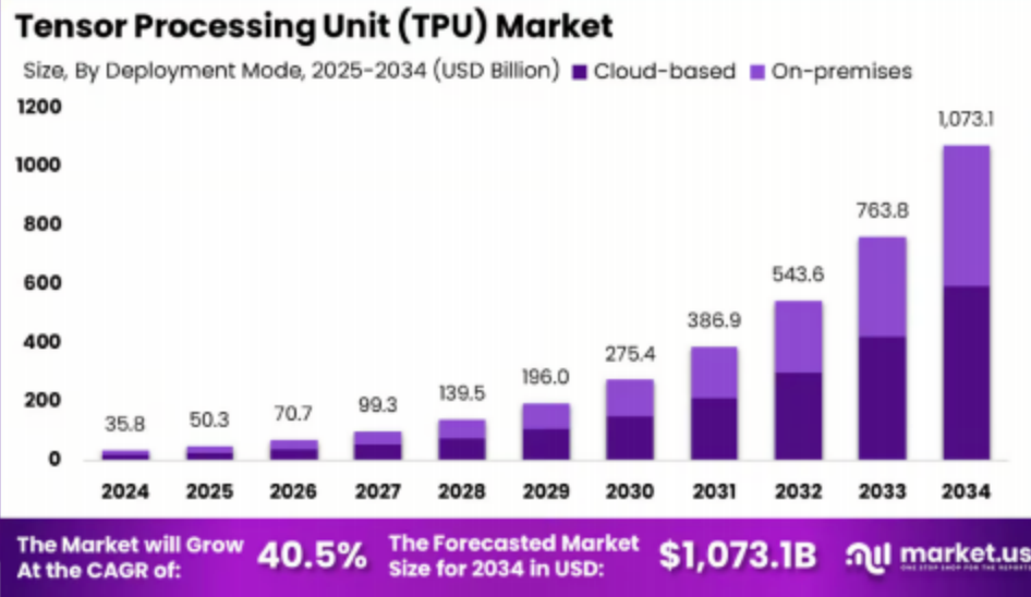
Market.us data shows that TPU will grow from 35.8 billion USD in 2024 to 107.3 billion USD in 2034, with a compound annual growth rate of up to 40.5%.
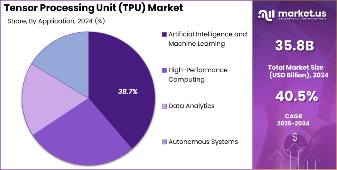
Market.us data shows that the global TPU market size in 2024 will be 35.8 billion USD, of which 38.7% is used for artificial intelligence and machine learning, with the remaining applications including high-performance computing, data analysis, and automation systems.
TPU market is divided into “Edge Edge TPU ” and “Cloud Cloud TPU“
Edge TPU is designed for AI inference at the device end, capable of real-time processing in compact and power-constrained environments. This type of TPU is increasingly being integrated into IoT devices, smart cameras, and industrial sensors, enabling organizations to process data at the source and respond instantly to dynamic changes. The adoption of edge computing in industries such as manufacturing, retail, and transportation is continuously increasing, driving the demand for edge TPU, as enterprises seek to enhance operational efficiency and customer experience through local intelligence.
Cloud TPU is optimized for large-scale AI training and inference tasks in centralized data centers. This type of TPU provides exceptional computing power, making it suitable for complex machine learning models, deep learning frameworks, and high-capacity data analysis.
Cloud service providers are continuously expanding their TPU-based product offerings, enabling enterprises to access AI infrastructure in a scalable and cost-effective manner without significant capital investment. The increasing reliance on cloud-based AI platforms for scientific research, product development, and business intelligence is a key factor driving the growth of the cloud TPU segment.
The synergy between edge TPU and cloud TPU is driving the rise of a hybrid AI deployment model, where initial data processing and inference can be completed at the edge, while more complex training and analysis are handled by the cloud.
Regional Markets
North America is the largest regional market for TPU globally, with a market size reaching 1.1 billion USD in 2024, accounting for approximately 39% of the global market. The region’s leading position is attributed to the concentration of large technology companies, strong investment in AI research and development, and a mature cloud computing ecosystem.
In particular, the United States is a core hub for AI hardware innovation, with leading cloud service providers and semiconductor companies driving the widespread application of TPU across multiple industries. It is expected that by 2033, the demand for TPU in North America will continue to grow at a compound annual growth rate of 19.8%, primarily driven by the continuous advancement of AI applications and infrastructure.
The Asia-Pacific region is rapidly emerging as the fastest-growing market for TPU, with a market size of 820 million USD in 2024. The rapid digitalization process, government policies promoting AI applications, and the expansion of data center infrastructure are key factors driving growth in this region.
Countries such as China, Japan, South Korea, and India are leading in AI innovation and are increasing investments in research, talent development, and ecosystem building. The Asia-Pacific TPU market is expected to grow at a compound annual growth rate of 24.2% during the forecast period, outpacing other regions and playing a significant role in global market expansion.
Europe also holds an important position in the global TPU market, with a market size of 600 million USD in 2024. The growth in this region is primarily driven by the widespread adoption of AI technologies in industries such as automotive, healthcare, and manufacturing. Governments and industry alliances in various European countries are actively supporting the construction of AI infrastructure and standards, creating a favorable environment for the application of TPU.
The Middle East and Africa and Latin America are gradually increasing their market share, with a combined market size of 280 million USD in 2024. These regions are accelerating the deployment of AI through smart city projects, digital transformation initiatives, and public-private partnerships. As regional markets continue to evolve, developing localized strategies and customized solutions will be key to seizing growth opportunities and addressing market differentiation.
Introduction to TPUCONTENT
The Tensor Processing Unit (TPU) is a dedicated chip developed by Google specifically for accelerating machine learning, excelling at executing large-scale matrix operations, particularly suitable for training and inference of neural networks; while Cloud TPU is its cloud-deployed version, allowing users to remotely access powerful TPU computing power through the Google Cloud platform without needing to own physical hardware, widely used for efficient training of AI tasks such as natural language processing and image recognition.
Version Iteration
First Generation: In 2015, Google began using the first generation TPU internally, an 8-bit matrix multiplication engine manufactured using a 28 nm process, with a die size of less than 331 mm², a clock speed of 700 MHz, and a thermal design power of 28–40 W. It is packaged with 8 GiB of dual-channel 2133 MHz DDR3 SDRAM, achieving a bandwidth of 34 GB/s.
Second Generation: The design of the first generation TPU was limited by memory bandwidth, so the second generation design used 16 GB of high-bandwidth memory, increasing the bandwidth to 600 GB/s, allowing performance to reach 45 TFLOPS. The TPU chip was then arranged into a four-chip module with a performance of 180 TFLOPS, and 64 such modules were assembled into a 256-chip Pod, achieving a performance of 11.5 PFLOPS.
Third Generation: In May 2018, Google announced that the performance of the third generation TPU was twice that of the second generation and would be deployed in Pods with four times the number of chips as the previous generation. Compared to the deployed second generation TPU, this increased the performance of each Pod by 8 times (with up to 1024 chips in each Pod).
Fourth Generation: In May 2021, Google announced that the performance of the fourth generation TPU was 2.7 times that of the third generation. Compared to the deployed third generation TPU, this increased the performance of each Pod by 5.4 times (with up to 4096 chips in each Pod).
Fifth Generation: In December 2023, Google launched TPU v5p, which is comparable in performance to NVIDIA’s H100.
Sixth Generation: In May 2024, Google launched TPU v6e Trillium. Google claims that TPU v6 can achieve a performance improvement of 4.7 times compared to TPU v5e, thanks to larger matrix multiplication units and faster clock speeds. The capacity and bandwidth of high-bandwidth memory (HBM) have both doubled.
Seventh Generation: In April 2025, at the Google Cloud Next conference, Google launched TPU v7 Ironwood. This new chip, named Ironwood, will have two versions: a cluster of 256 chips and a cluster of 9,216 chips. The peak computing capability of Ironwood can reach 4614 TFLOPS.
 Comparison of TPU with CPU and GPUCONTENT
TPU is a processor designed specifically for machine learning tasks, particularly excelling in tensor calculations and large-scale matrix operations in deep learning, demonstrating outstanding performance in speed and efficiency. Its architecture is highly specialized, allowing it to far exceed other processors when handling AI models, making it suitable for specific scenarios requiring high-performance computing.
GPU has powerful parallel processing capabilities and is widely used in graphics rendering, gaming, and some machine learning tasks. Although it is not as specialized in AI as TPU, it performs well in multitasking, balancing speed and flexibility, making it an ideal choice between general computing and high-performance demands.
CPU is the most general-purpose processor, supporting almost all types of software and computing tasks, with high flexibility and wide applicability. However, its performance in parallel processing and machine learning is inferior to that of TPU and GPU, making it more suitable for executing traditional computing and control logic tasks.
Comparison of Working Principles
CPU
CPU is a general-purpose processor based on the von Neumann architecture. This means that the CPU works in conjunction with software and memory. The greatest advantage of CPUs is their flexibility. You can load any type of software for many different types of applications on a CPU. You can use a CPU for word processing on a PC, controlling rocket engines, processing bank transactions, or classifying images through neural networks.
For each computation, the CPU loads values from memory, performs calculations on those values, and then stores the results back in memory. Compared to computation speed, memory access speed is slower and may limit the overall throughput of the CPU. This is often referred to as the von Neumann bottleneck.
CPU Working Principle Diagram
Comparison of Working Principles
GPU
To improve throughput, GPU contains thousands of arithmetic logic units (ALUs) within a single processor. Most GPUs typically contain between 2500 and 5000 ALUs. The large number of processors means you can perform thousands of multiplications and additions simultaneously. This GPU architecture is very suitable for parallel processing of large computations – applications in matrix operations in neural networks.
In fact, on typical training workloads used for deep learning, the throughput of GPU is an order of magnitude higher than that of CPU. However, GPU is still a general-purpose processor that must support many different applications and software. Therefore, GPU faces the same issues as CPU. For each computation among thousands of ALUs, the GPU must access registers or shared memory to read operands and store intermediate results.
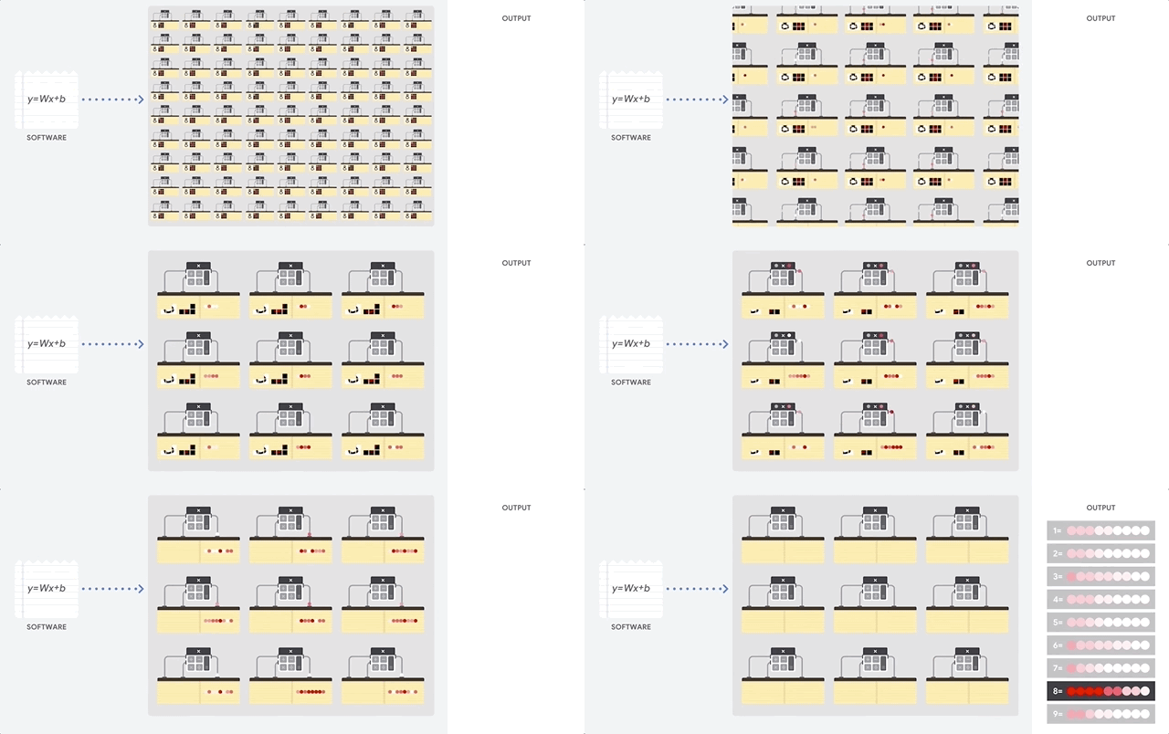
GPU Working Principle Diagram
TPU
Google designed Cloud TPU, which are matrix processors specifically for neural network workloads. TPUs cannot run word processors, control rocket engines, or perform bank transactions, but they can quickly process the large number of matrix operations used in neural networks. TPU ‘s main task is matrix processing, which is a combination of multiplication and accumulation operations.
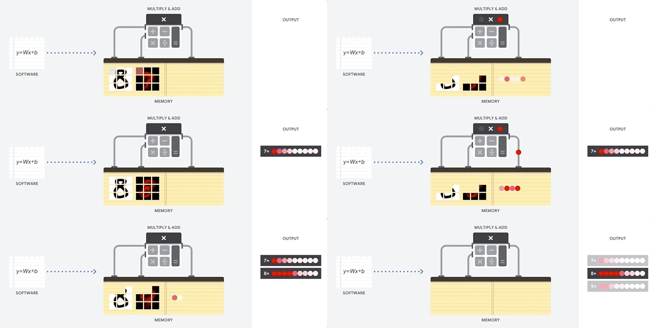
TPUs contain thousands of multiply-accumulate units that are directly connected to form large physical matrices. This is called a systolic array architecture. TPU hosts stream data into feed-in queues. TPU loads data from the feed-in queue and stores it in HBM memory. After computation is complete, TPU loads the results into the feed-out queue. Then, TPU hosts read the results from the feed-out queue and store them in the host’s memory.
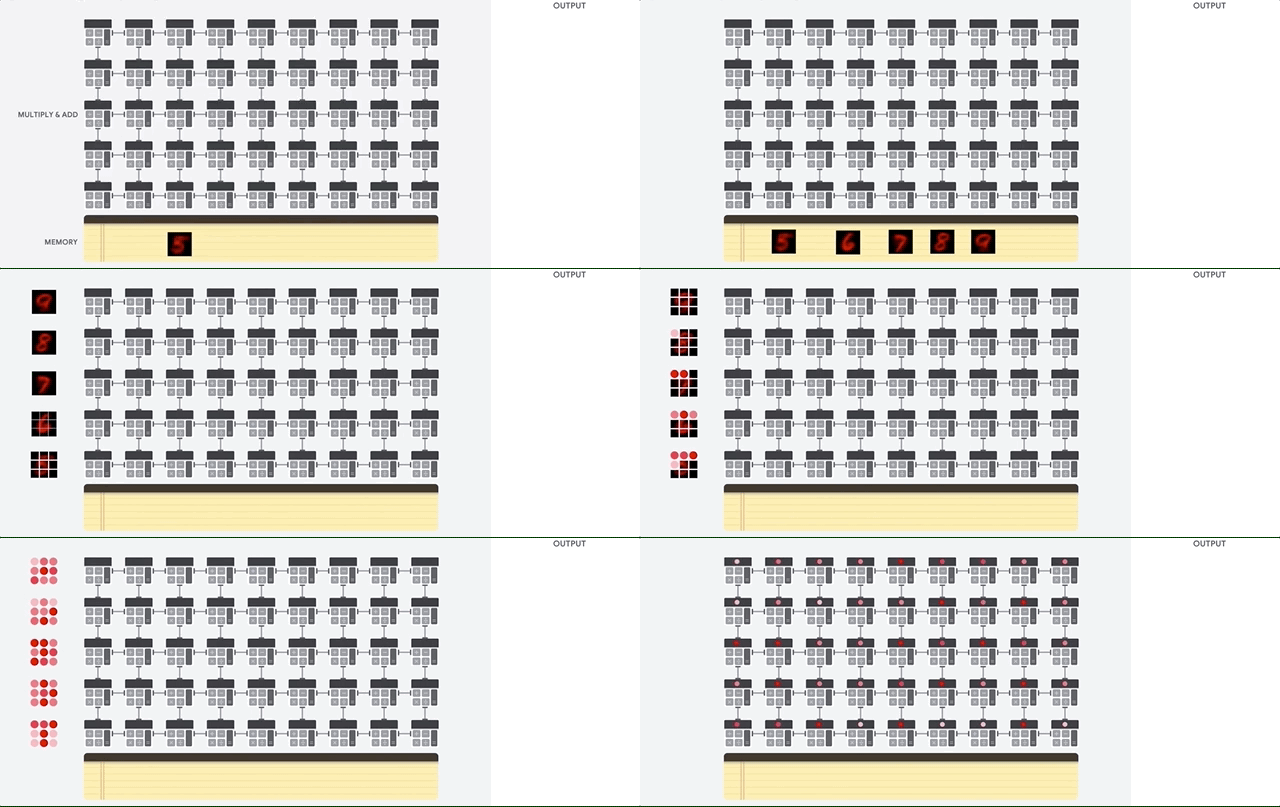
TPU Working Principle Diagram. To perform matrix operations, TPU loads parameters from HBM memory into the matrix multiplication unit MXU.
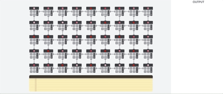
Then, TPU loads data from memory. Each time a multiplication operation is performed, the system passes the result to the next multiply-accumulate unit. The output is the sum of all multiplication results between the data and parameters. During the matrix multiplication process, there is no need to access memory. Therefore, TPU can achieve high computational throughput in neural network calculations.
Comparison of TPU with NPUCONTENT
NPU and TPU Current and Future Application Areas
Cloud Computing: Both NPU and TPU can be used to provide cloud-based AI services – image recognition, natural language processing, and speech synthesis. Google Cloud offers AI services based on TPU – Cloud Vision, Cloud Natural Language, and Cloud Text-to-Speech.
Edge Computing: Both NPU and TPU can be used to support edge-side AI applications – facial recognition, voice control, and gesture recognition. Huawei’s Kirin 990 chip integrates NPU, enabling edge AI applications on devices such as smartphones.
Assisted Driving: Both NPU and TPU can be used to support assisted driving systems – object detection, lane recognition, and path planning. Tesla’s assisted driving chip uses NPU, capable of processing 2300 frames per second and supporting 12 cameras and 8 radars.
Healthcare: Both NPU and TPU can be used to enhance healthcare services – disease diagnosis, treatment, and health monitoring. Google’s Health TPU can help detect diseases such as diabetic retinopathy and breast cancer through medical imaging.
NPU and TPU Various Differences
Architecture: NPU adopts the traditional von Neumann architecture, separating memory from processing units; while TPU adopts a systolic array architecture, integrating memory and processing units on the same chip.
Performance: NPU typically has higher peak performance than TPU, but its latency and power consumption are also higher; TPU has slightly lower peak performance but performs better in terms of latency and energy efficiency.
Cost: Due to more complex designs and more components, NPU is more expensive than TPU; TPU has a simpler structure and requires fewer components, thus having a lower cost.
Availability: NPU is produced by multiple manufacturers – Intel, NVIDIA, Huawei, and Samsung, with broader market supply; while TPU is produced only by Google, making its availability relatively low.
NPU and TPU Pros and Cons Comparison
NPU
Advantages: NPU has higher peak performance than TPU, meaning it can handle more complex and diverse neural networks.
Disadvantages: NPU has higher latency and power consumption than TPU, running slower and at a higher cost.
TPU
Advantages: TPU has lower latency and power consumption than NPU, running faster and more efficiently.
Disadvantages: TPU has lower peak performance than NPU, suitable only for specific and highly optimized neural networks.
TPU ArchitectureCONTENT
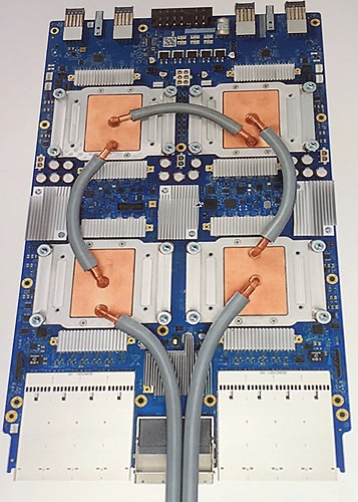
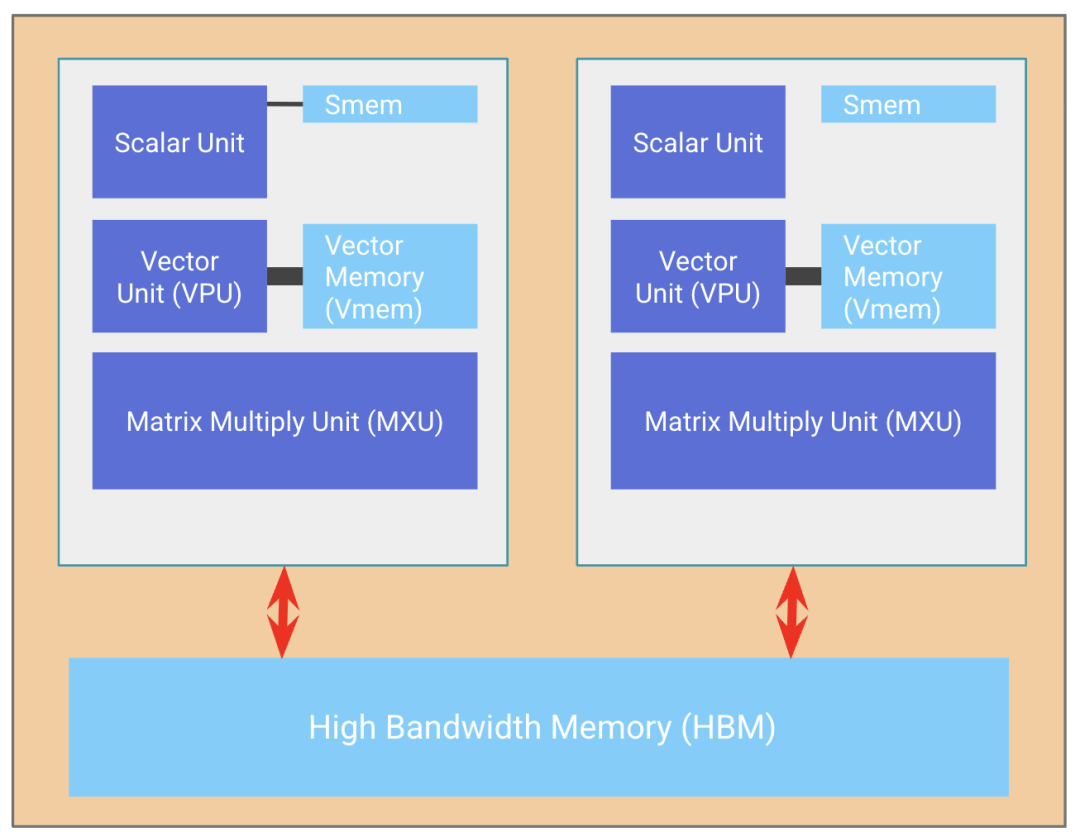
TPU is a computing unit centered on matrix multiplication tasks TensorCore, with integrated high-speed stacked memory HBM to support large-scale tensor operations.
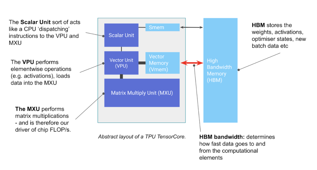
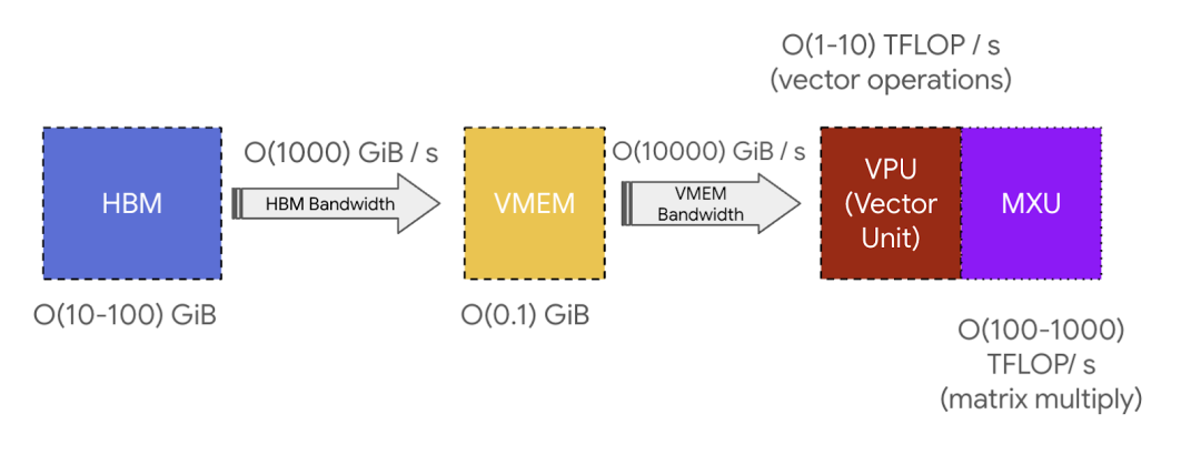
The basic components of the TPU chip – TensorCore is the gray module on the left, which contains matrix multiplication units MXU, vector processing units VPU, and vector memory VMEM.
Matrix Multiplication UnitMXU is an important component of TensorCore. In most TPU generations, it executes a systolic array operation every 8 cycles using bfloat16[8,128] @ bf16[128,128], outputting f32[8,128]. On TPU v5e, a single MXU at 1.5GHz has a computational capacity of approximately 5e13 bfloat16 FLOPs/s.
Most TensorCores contain 2 or 4 MXUs, so for example, TPU v5e’s total bfloat16 floating-point computation capacity is approximately 2e14 FLOPs/s. TPU also supports lower precision matrix multiplication operations to achieve higher throughput. For instance, each TPU v5e chip can execute approximately 4e14 int8 OPs/s.
Vector Processing UnitVPU is responsible for executing general mathematical operations – ReLU activation functions, pointwise addition or multiplication operations between vectors. Vector reduction operations are also completed in this unit.
Vector MemoryVMEM is an on-chip cache located within TensorCore, close to the computing units. Its capacity is much smaller than that of HBM, but it has higher bandwidth with respect to the MXU. The operation of VMEM is similar to that of L1/L2 caches in CPUs, but with larger capacity and programmer control. Before any computation is executed in TensorCore, data from HBM must first be copied to VMEM.
High Bandwidth MemoryHBM is a high-speed, large-capacity memory used to store tensor data for TensorCore. The capacity of HBM is typically in the tens of GiB – TPU v5e is equipped with 16GiB of HBM. When computation is needed, tensors flow from HBM through VMEM into the MXU, and the computation results are written back from VMEM to HBM.
The bandwidth between HBM and TensorCore is referred to as HBM bandwidth, typically around 1–2TB/s. This bandwidth determines the speed limit of computation in memory-constrained tasks.
VMEM and Arithmetic Intensity: The capacity of VMEM is much smaller than that of HBM, but its bandwidth with the MXU (matrix multiplication unit) is much higher. As mentioned in Section 1, if the input/output data of an algorithm can fully fit into VMEM, it is unlikely to encounter communication bottlenecks.
This is especially important for computations with low arithmetic intensity: the bandwidth of VMEM is approximately 22 times that of HBM, meaning that the MXU can achieve peak FLOPs utilization with only 10–20 arithmetic intensity when reading or writing data from VMEM.
This means that if we can place weights in VMEM instead of HBM, matrix multiplication can reach computational bottlenecks (FLOPs bound) with smaller batch sizes. It also means that algorithms with inherently low arithmetic intensity can still run efficiently. The only challenge is that the capacity of VMEM is very small.
A TPU chip typically contains two TPU cores, which share memory and can be viewed as a large accelerator with double the FLOPs, a configuration known as a megacore. This architecture has become standard since TPU v4. Earlier TPU chips – TPU v3 and earlier versions – used independent memory and were viewed as two separate accelerators. The inference-optimized chip TPU v5e contains only one TPU core per chip.
Chips are typically arranged in groups of 4 on a tray and connected to a CPU host via a PCIe network. This is the configuration most readers are familiar with: 4 chips – a total of 8 cores, but usually regarded as 4 logical megacores, accessible via Colab or a single TPU-VM. For inference-optimized chips – TPU v5e, each host connects to two trays instead of one, but each chip contains only one core, resulting in a total of 8 chips / 8 cores.
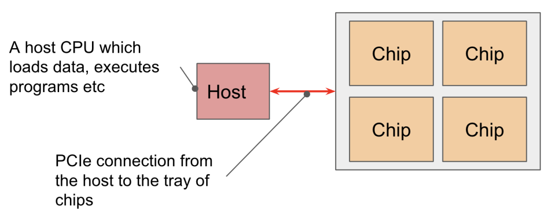
PCIe bandwidth is limited: just like the connection between HBM and VMEM, the PCIe interface between the CPU and HBM also has specific bandwidth limitations, which restrict the speed of loading from host memory to HBM or back from HBM. For example, TPU v4 has a PCIe bandwidth of 16GB/second in each direction, which is nearly 100 times slower than HBM. Users can load or unload data to the host CPU memory, but the speed is not fast.
TPU Cloud ArchitectureCONTENT
Google Cloud can use TPU VM virtual machines as computing resources. You can directly use TPU VM for workloads or use it through Google Kubernetes Engine or Vertex AI with TPU VM.
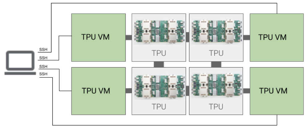
TPU VM virtual machine architecture allows users to connect directly via SSH to virtual machines physically connected to TPU chips. These virtual machines run a Linux system, have access to the underlying TPU, and grant users full root permissions to execute arbitrary code. Users can directly view compiler outputs, runtime logs, and debugging information, allowing for more flexible control and optimization of AI workloads.
TPU hosts are virtual machines deployed on physical computing nodes connected to TPU hardware. Workloads can choose different host configurations based on scale and demand: single host configuration uses only one TPU virtual machine; multi-host configuration distributes training tasks across multiple virtual machines; sub-host configuration uses only part of the TPU chip resources on the virtual machine, suitable for lightweight or shard tasks.
The value of TPU has transcended the hardware itself – it has become a benchmark for measuring the speed of AI penetration. From medical imaging to consumer terminals, this debate over the scope of computing power deployment will determine the direction of the technological competition in the next decade.
Recommended Reading
In-depth Comparison of Cabin Chip CPU Architecture and Scene Functions: x86 Architecture AMD vs. ARM Architecture Qualcomm Snapdragon 8295
A Detailed Explanation of Domestic GPU Leader – Muxi Technology
The Industrial Process and Product Technology of Domestic GPU Star Company – Birun Technology
Technical Breakthroughs and Product Layout of Domestic GPU Giant – Moer Thread
Vehicle Networking SOC Chip Technology Solutions and Development Trends
—end—