
Introduction: Chips are formed through a series of operations including the design, manufacturing, and packaging of integrated circuits. Generally speaking, integrated circuits focus more on the design and layout of the circuits, while chips pay more attention to the integration, production, and packaging of the circuits. However, in everyday life, the terms “integrated circuit” and “chip” are often used interchangeably.
The Complex and Tedious Chip Design Process
The chip manufacturing process is akin to building a house with LEGO bricks; it starts with a wafer as the foundation, and then the layers of the chip manufacturing process are stacked upon it to produce the necessary IC chips (which will be introduced later). However, without a design blueprint, even the strongest manufacturing capabilities are useless; thus, the role of the architect is crucial. But who exactly is the architect in IC design? This article will introduce IC design next.
In the IC production process, ICs are often planned and designed by specialized IC design companies. Well-known companies like MediaTek, Qualcomm, and Intel design their own IC chips, providing different specifications and performances for downstream manufacturers to choose from. Since ICs are designed by various companies, IC design heavily relies on the skills of engineers, and the quality of engineers affects the value of a company. However, what steps do engineers take when designing an IC chip? The design process can be simply divided into the following steps.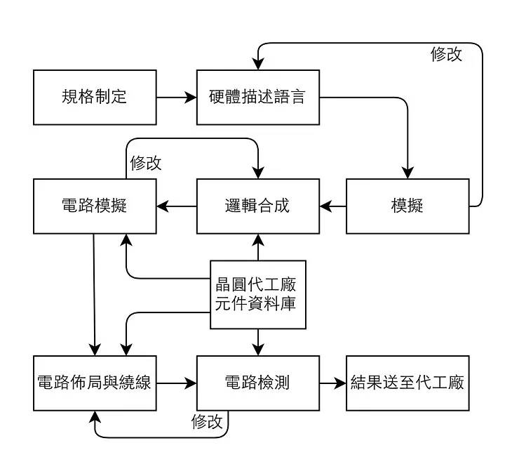
The First Step in Design: Setting Goals
In IC design, the most important step is specification formulation. This step is akin to deciding how many rooms and bathrooms are needed before designing a building. There are also regulations that need to be followed. Once all functions are confirmed, the design can proceed without the need for additional modifications later. IC design requires a similar process to ensure that the designed chip has no errors.
The first step in specification formulation is to determine the purpose and performance of the IC, setting the overall direction. Next, it is necessary to check which agreements need to be met. For example, a chip for a wireless network card must comply with IEEE 802.11 standards, otherwise, the chip will not be compatible with products on the market, making it impossible to connect with other devices. Finally, the implementation method of this IC is established, with different functions assigned to different units, and the connection methods between different units are determined, thus completing the specification formulation.
After completing the specifications, the next step is to design the details of the chip. This step is like sketching the initial plan of a building, outlining the overall structure for easier subsequent drafting. In IC chips, hardware description languages (HDL) are used to describe the circuits. Commonly used HDLs include Verilog and VHDL, through which the functionality of an IC can be easily expressed in code. The next step is to check the correctness of the program’s functionality and continue to modify it until it meets the expected functionality.
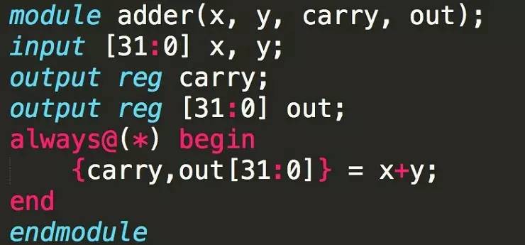 ▲ Example of a 32-bit adder in Verilog.
With Computers, Things Become Easier
With a complete plan, the next step is to draw the flat design blueprint. In IC design, the logic synthesis step takes the verified HDL code and inputs it into electronic design automation (EDA) tools, allowing the computer to convert the HDL code into logic circuits, producing circuit diagrams as shown below. After that, the logic gate design diagram is repeatedly verified against the specifications and modified until the functionality is correct.
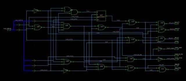 ▲ Result after synthesizing the control unit.
Finally, the synthesized code is input into another set of EDA tools for circuit layout and routing (Place And Route). After continuous testing, the following circuit diagram will be formed. In the diagram, different colors represent different masks. How are these masks used?
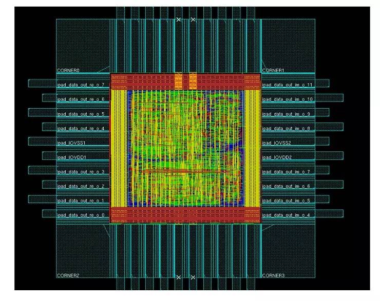 ▲ Commonly used calculation chip – FFT chip, completed circuit layout and routing results.
Layered Masks Stack Up to Form a Chip
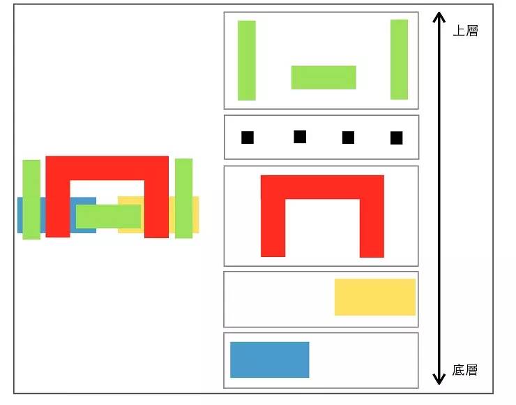
First, it is now known that an IC will generate multiple masks, which have upper and lower layers, each with its own tasks. The following diagram is a simple example of a mask, taking the basic component CMOS in integrated circuits as an example. CMOS stands for Complementary Metal-Oxide-Semiconductor, which combines NMOS and PMOS to form CMOS. What is a metal-oxide-semiconductor (MOS)? This component, widely used in chips, is somewhat difficult to explain, and general readers may find it hard to understand, so we will not delve into it here.
In the diagram, the left side shows the circuit diagram formed after layout and routing. As previously mentioned, each color represents a mask. The right side shows how each mask is laid out. The manufacturing process starts from the bottom layer, following the methods described in the previous IC chip manufacturing process, layer by layer, until the desired chip is produced.
 At this point, there should be a preliminary understanding of IC design. Overall, it is clear that IC design is a very complex specialty, and thanks to the maturity of computer-aided software, IC design can be accelerated. IC design companies heavily rely on the intelligence of engineers, and each step described here requires specialized knowledge, which can independently form multiple specialized courses, such as writing hardware description languages, which not only requires familiarity with programming languages but also an understanding of how logic circuits work, how to translate the required algorithms into code, and how synthesis software converts code into logic gates, among other issues.
What is a Wafer?
In semiconductor news, we often hear about wafer fabs designated by size, such as 8-inch or 12-inch fabs. However, what exactly is a wafer? What does the 8-inch refer to? What difficulties are involved in producing large-sized wafers? Below, we will gradually introduce the most important foundation of semiconductors – what exactly is a “wafer”.
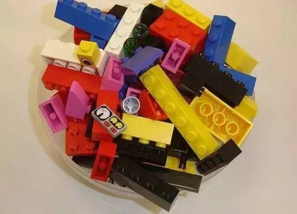
A wafer is the foundation for manufacturing various computer chips. We can liken chip manufacturing to building a house with LEGO bricks, where layers are stacked to complete the desired shape (various chips). However, without a good foundation, the house will be crooked and not fit for purpose; to create a perfect house, a stable substrate is needed. For chip manufacturing, this substrate is the wafer described next.
 (Source: Flickr/Jonathan Stewart CC BY 2.0)
First, recall when playing with LEGO bricks as a child, the surface of the bricks has small round protrusions that allow two bricks to be securely stacked without glue. Chip manufacturing also uses a similar method to securely attach the subsequent atoms and substrate. Thus, we need to find a substrate with a smooth surface to meet the requirements for subsequent manufacturing.
Among solid materials, there is a special crystalline structure – monocrystalline. It has the characteristic of atoms being tightly arranged one after another, forming a smooth atomic surface. Therefore, using monocrystalline to make wafers can meet the above requirements. However, how can such materials be produced? There are primarily two steps: purification and crystal pulling, which will complete such materials.
How to Manufacture Monocrystalline Wafers
Purification is divided into two stages. The first step is metallurgical-grade purification, where carbon is added to convert silicon dioxide into silicon with over 98% purity through a reduction reaction. Most metal refining, such as iron or copper, is obtained through this method to achieve sufficient metal purity. However, 98% purity is still not enough for chip manufacturing and needs further enhancement. Therefore, the Siemens process is used for purification, thus obtaining high-purity polysilicon required for semiconductor processes.
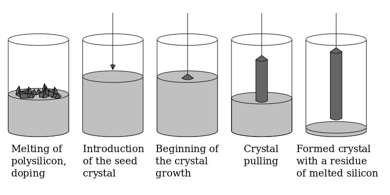 ▲ Silicon rod manufacturing process (Source: Wikipedia)
Next is the crystal pulling step. First, the previously obtained high-purity polysilicon is melted to form liquid silicon. Then, a seed of single-crystal silicon comes into contact with the liquid surface and is slowly pulled upward while rotating. The reason for needing a single-crystal silicon seed is that the arrangement of silicon atoms is similar to people lining up; a leader is needed to guide the subsequent atoms in proper arrangement. The silicon seed serves as this leader, showing the later atoms how to line up correctly. Finally, once the silicon atoms solidify after leaving the liquid surface, a neatly arranged single-crystal silicon rod is completed.
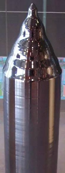 ▲ Single-crystal silicon rod (Source: Wikipedia)
However, what do the 8-inch and 12-inch refer to? They refer to the diameter of the thin circular slices obtained from the silicon rods after processing and cutting. Why is it more challenging to manufacture large-sized wafers? As mentioned earlier, the process of making silicon rods is akin to making cotton candy, where the rod is formed while rotating. Those who have made cotton candy know that producing large and solid cotton candy is quite difficult, and the same goes for crystal pulling; the speed of rotation and temperature control during the pulling process will affect the quality of the rod. Therefore, the larger the size, the higher the requirements for speed and temperature during crystal pulling. Hence, producing high-quality 12-inch wafers is more challenging than 8-inch wafers.
However, a complete silicon rod cannot be used as the substrate for chip manufacturing. To create thin silicon wafers, the silicon rods need to be cut into circular slices using diamond blades, and the slices are polished to form the silicon wafers required for chip manufacturing. After so many steps, the manufacturing of the chip substrate is successfully completed, and the next step is to stack the layers to create the chip. How are chips made?
Layered Stacking to Build Chips
After introducing what silicon wafers are, we also know that manufacturing IC chips is like building a house with LEGO bricks, where layers are stacked to create the desired shape. However, building a house involves many steps, and IC manufacturing is no different. What are the steps involved in manufacturing ICs? This article will introduce the process of IC chip manufacturing.
Before starting, we need to understand what an IC chip is. IC, short for Integrated Circuit, as its name suggests, combines the designed circuits in a stacked manner. By this method, we can reduce the area required for connecting circuits. The following diagram shows a 3D view of an IC circuit, where the structure resembles the beams and columns of a house, stacked layer upon layer, which is why IC manufacturing is likened to building a house.
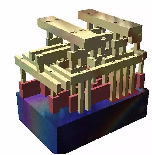 ▲ 3D cross-section of an IC chip. (Source: Wikipedia)
From the above 3D cross-section of the IC chip, the deep blue part at the bottom is the wafer introduced in the previous section. This image clearly shows the important role that the wafer substrate plays in the chip. The red and tan parts are the areas to be completed during IC production.
First, the red area can be likened to the lobby of a high-rise building. The lobby serves as the entrance to a building, where all traffic flows in and out, and it typically has more functionality than other floors. Therefore, compared to other floors, the construction is more complex and requires more steps. In the IC circuit, this lobby is the logic gate layer, which is the most crucial part of the entire IC, combining various logic gates to complete a fully functional IC chip.
The yellow parts are like regular floors. Compared to the lobby, they do not have overly complex structures, and there are not many changes during construction. The purpose of this layer is to connect the logic gates of the red part. The reason for needing so many layers is that there are too many lines to connect, and if a single layer cannot accommodate all the lines, multiple layers must be stacked to achieve this goal. In this process, the lines of different layers will connect vertically to meet the wiring needs.
Layered Construction, Building Up Gradually
After understanding the structure of the IC, the next step is to introduce how to manufacture it. Imagine if you were to create intricate designs using a spray paint can, you would first need to cut out a stencil to cover the paper. Then, you would evenly spray paint over the paper, and once the paint dries, you would remove the stencil. By continuously repeating this process, you can create neat and complex patterns. IC manufacturing follows a similar approach, stacking layers through masking.
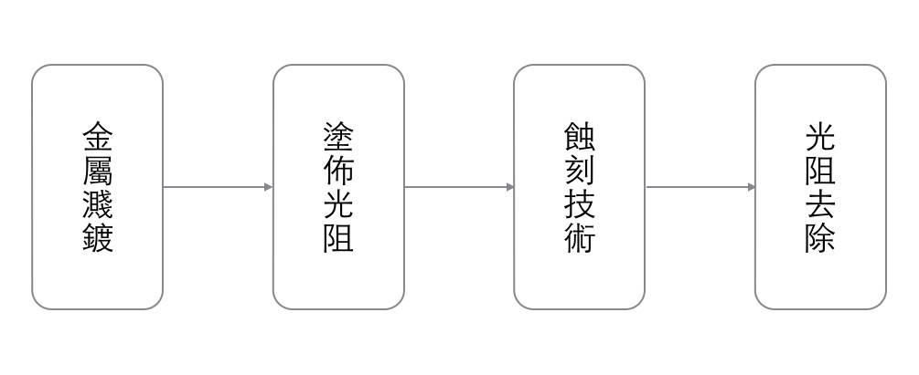
The IC manufacturing process can be simply divided into the above four steps. Although the actual manufacturing steps may vary and the materials used may differ, they generally follow similar principles. This process differs slightly from painting; in IC manufacturing, the coating is applied first, followed by masking, while in painting, masking is done before painting. The following describes each process.
Metal Sputtering: The desired metal material is evenly sprinkled on the wafer to form a thin film.
Photoresist Coating: First, the photoresist material is placed on the wafer, and by using a mask (the principle of masks will be explained later), light beams are directed onto the unwanted areas to damage the structure of the photoresist material. Then, a chemical agent is used to wash away the damaged material.
Etching Technology: The silicon wafer that is not protected by the photoresist is etched using an ion beam.
Photoresist Removal: A photoresist remover is used to dissolve the remaining photoresist, thus completing one cycle of the process.
Finally, many IC chips will be completed on an entire wafer, and the completed square IC chips can be cut out and sent to packaging factories for packaging. What are packaging factories? This will be explained later.
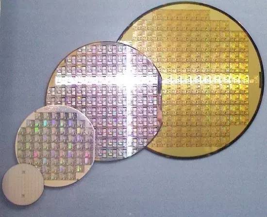 ▲ Comparison of various wafer sizes. (Source: Wikipedia)
What is Nanometer Process?
Samsung and TSMC are fiercely competing in advanced semiconductor processes, both aiming to seize an advantage in wafer foundry to secure orders, leading to a near war over 14nm and 16nm processes. However, what do these numbers really mean, and which parts do they refer to? What benefits and challenges arise from reducing the process size? Below, we will provide a brief explanation of the nanometer process.
How Small is a Nanometer?
Before starting, it is essential to understand what a nanometer is. In mathematics, a nanometer is 0.000000001 meters, but this is a rather abstract example, as we can only see a lot of zeros after the decimal point without any real feeling. A more tangible comparison would be the thickness of a fingernail.
Measuring with a ruler reveals that the thickness of a fingernail is approximately 0.0001 meters (0.1 millimeters), which means if you were to cut a fingernail’s side into 100,000 lines, each line would be about 1 nanometer. This gives a rough idea of how small a nanometer is.
Now that we know how small a nanometer is, we must understand the purpose of reducing the process size. The primary goal of shrinking transistors is to fit more transistors into a smaller chip, preventing chips from becoming larger as technology improves. Additionally, it can increase the processing efficiency of the processor; furthermore, reducing the size can lower power consumption; finally, a smaller chip is easier to fit into mobile devices, meeting future demands for thinner and lighter designs.
Returning to the nanometer process, taking 14nm as an example, this process means that the smallest line in the chip can be as small as 14 nanometers in size. The following image shows the appearance of traditional transistors, which serves as an example. The main purpose of shrinking transistors is to reduce power consumption, but which part should be reduced to achieve this? The L in the lower left image is the part we aim to shrink. By shortening the gate length, the current can take a shorter path from the Drain to the Source (if interested, you can search for MOSFET on Google for a more detailed explanation).
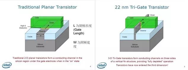 (Source: www.slideshare.net)
Furthermore, computers operate using 0s and 1s; how do transistors meet this requirement? The method is to determine whether current flows through the transistor. When voltage is supplied at the Gate (the green square), current will flow from the Drain to the Source; if no voltage is supplied, current will not flow, thus representing 1 and 0. (If interested in why we use 0 and 1 for judgment, you can look up Boolean algebra; this method is used to create computers.)
There Are Physical Limits to Size Reduction
However, the process cannot be reduced indefinitely. When we shrink transistors to around 20 nanometers, we encounter issues from quantum physics, leading to leakage current in transistors, offsetting the benefits gained from reducing L. One way to improve this is to introduce the FinFET (Tri-Gate) concept, as shown in the upper right image. In Intel’s previous explanations, it can be seen that by adopting this technology, leakage phenomena caused by physical issues can be reduced.
(Source: www.slideshare.net)
More importantly, this method can increase the contact area between the Gate and the lower layer. In traditional methods (left upper image), the contact area is only a flat surface, but by adopting FinFET (Tri-Gate) technology, the contact area becomes three-dimensional, easily increasing the contact area, thus significantly aiding in size reduction while maintaining the same contact area.
Finally, why is it said that major manufacturers face severe challenges when entering the 10nm process? The main reason is that the size of a single atom is about 0.1 nanometers, and at 10 nanometers, a line consists of less than 100 atoms. This makes production extremely challenging, and if there is a defect in a single atom, such as an atom falling out during production or the presence of impurities, it can result in unknown phenomena, affecting the yield of the product.
If you cannot imagine this difficulty, you can conduct a small experiment. Arrange 100 small beads into a 10×10 square on a table and cover them with a sheet of paper. Then use a small brush to sweep away the beads around the edges, leaving a 10×5 rectangle. This will illustrate the difficulties faced by major manufacturers and how arduous it is to achieve this goal.
As Samsung and TSMC recently completed mass production of 14nm and 16nm FinFET processes, both are vying for Apple’s next-generation iPhone chip foundry, and we will witness exciting commercial competition, while also gaining more power-efficient and thinner phones, thanks to the benefits brought by Moore’s Law.
What is Packaging?
After a long process from design to manufacturing, we finally obtain an IC chip. However, a chip is quite small and thin; without external protection, it can be easily scratched or damaged. Additionally, due to the small size of the chip, it would be difficult to manually place it on a circuit board without a larger shell. Therefore, this article will now describe packaging.
Currently, there are two common packaging methods: one is the DIP package, commonly seen in electric toys, resembling a black centipede, and the other is the BGA package, commonly seen when purchasing boxed CPUs. Other packaging methods include PGA (Pin Grid Array) used in early CPUs or QFP (Quad Flat Package), an improved version of DIP. Due to the numerous packaging methods, we will introduce DIP and BGA packaging.
Traditional Packaging: Timeless and Enduring
First, we will introduce the Dual Inline Package (DIP). As seen in the diagram below, IC chips using this packaging have dual rows of pins, making them look like black centipedes, leaving a deep impression. This packaging method is the earliest adopted IC packaging technology, offering the advantage of low cost, suitable for small chips that do not require many connections. However, since most are made of plastic, the heat dissipation is poor, failing to meet the requirements of current high-speed chips. Therefore, those using this packaging are mostly classic chips, such as OP741 in the diagram below, or IC chips that are smaller and do not require high operational speeds.
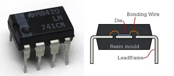 ▲ The IC chip on the left is OP741, a common voltage amplifier. The right image is its cross-section, where the packaging connects the chip to the metal leadframe using gold wire. (Source: Left image Wikipedia, Right image Wikipedia)
The BGA (Ball Grid Array) packaging, compared to DIP, has a smaller body and can be easily placed in smaller devices. Additionally, since the pins are located underneath the chip, it can accommodate more metal pins compared to DIP, making it suitable for chips that require more connections. However, this packaging method is more expensive, and the connection process is more complex, thus it is primarily used in high-priced products.
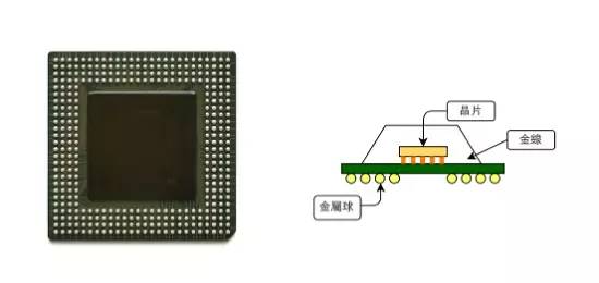 ▲ The left image shows a chip using BGA packaging. The right image is a schematic diagram of BGA packaging using flip-chip technology. (Source: Left image Wikipedia) Mobile devices have emerged, and new technologies have taken the stage.
However, using the above packaging methods consumes a considerable amount of space. Current mobile devices and wearable devices require a variety of components, and if each component is independently packaged, it will take up a significant amount of space. Therefore, there are currently two methods to meet the size reduction requirements: SoC (System On Chip) and SiP (System In Package).
When smartphones first emerged, the term SoC was frequently seen in major financial magazines. But what exactly is SoC? In simple terms, it is the integration of originally different functional ICs into a single chip. This method not only reduces size but also shortens the distance between different ICs, enhancing the chip’s processing speed. The method of production involves placing various different ICs together during the IC design phase and then using the previously described design process to create a mask.
However, SoC is not without its drawbacks. Designing an SoC requires a considerable amount of technical collaboration. When IC chips are packaged separately, each has external protection, and the distance between ICs is relatively far, minimizing the chances of cross-interference. However, when all ICs are packaged together, it becomes a nightmare. IC design companies must transition from simply designing ICs to understanding and integrating the functions of various ICs, increasing the workload for engineers. Additionally, many situations may arise, such as high-frequency signals from communication chips potentially affecting other functional ICs.
Furthermore, SoC also requires obtaining IP (intellectual property) licenses from other manufacturers to incorporate designed components into the SoC. This means that complete design details of the entire IC must be obtained to create a complete mask, which also increases the design costs for SoC. Some may question why not design a new one instead? The reason is that designing various ICs requires a wealth of knowledge related to those ICs, and only financially robust companies like Apple can afford to hire top engineers from well-known companies to design an entirely new IC. Collaborating through licensing is still more cost-effective than self-developing.
A Compromise: SiP Emerges
As an alternative, SiP has taken the stage in integrated chips. Unlike SoC, it involves purchasing ICs from various manufacturers and packaging them together in the final stage, thus eliminating the need for IP licensing and significantly reducing design costs. Additionally, since they are independent ICs, the level of interference between them is greatly reduced.
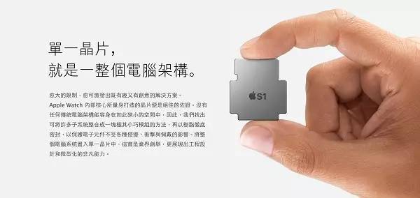 ▲ The Apple Watch uses SiP technology to encapsulate the entire computer architecture into a single chip, not only meeting performance expectations but also reducing size, allowing more space for batteries. (Source: Apple Official Website)
The most notable product utilizing SiP technology is undoubtedly the Apple Watch. Due to the limited internal space of the watch, traditional techniques could not be used, and the design costs of SoC were too high, making SiP the primary choice. By using SiP technology, not only can the size be reduced, but the distance between various ICs can also be shortened, making it a feasible compromise. The following diagram shows the internal configuration of the S1 chip used in the Apple Watch, which includes many ICs.
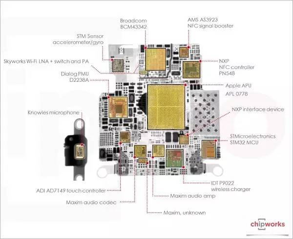 ▲ Internal configuration diagram of the S1 chip using SiP packaging in the Apple Watch. (Source: chipworks)
After packaging is complete, the next phase is testing, which involves confirming whether the packaged IC operates normally. Once verified, it can be shipped to assembly factories to create the electronic products we see. At this point, the semiconductor industry has completed the entire production task.
Top Ten IDM Companies:
1. Intel (acquired Altera)
2. Samsung
3. SK Hynix
4. Micron (acquired Elpida)
5. Texas Instruments (TI) (acquired National Semiconductor)
6. NXP (acquired Freescale)
7. Toshiba
8. Infineon (acquired IR)
9. STMicroelectronics
10. Sony
Fabless Companies (pure design, no wafer fab):
Qualcomm
Avago (acquired Broadcom)
MediaTek (MTK)
NVIDIA
AMD
Shenzhen HiSilicon
Apple
Analog Devices (ADI) (acquired Linear)
Renesas
Marvell
Xilinx
Spreadtrum
ON Semiconductor (acquired Fairchild, Aptina)
ROHM Semiconductor
Novatek
Dialog Semiconductor
Realtek
Himax
Cirrus Logic
Lattice
Datang Semiconductor
China Huada
Yili
Dynex
ZTE
Rockchip
Allwinner
ACTIONS
Gekowe Micro
Goodix Technology
Silicon Labs
National Chip
Guokong Technology
Junzheng
Lanqi
Yingfangwei
Silicon Labs
…and many more
Wafer Foundries:
1. TSMC
2. GlobalFoundries (merged with IBM’s IC business and Singapore’s CSM)
3. UMC
4. Samsung
5. SMIC
6. Powerchip
7. Tower Jazz
8. Fujitsu
9. Vanguard Semiconductor
10. HHNEC
11. Dongbu
12. SSMC
13. WIN
14. PSC
15. VIS
16. MagnaChip
17. CSMC
18. TJSemi
19. Jilin Huamei
20. HLMC
21. Changjiang Storage (Wuhan Xinxin, Unisoc)
22. Wuxi SK Hynix STMicroelectronics
23. Intel Semiconductor (Dalian)
24. ASMC
25. HJT Technology (Suzhou) (HJTC)
26. Tianshui Tian Guang
27. Shenzhen Fangzheng Micro
28. Hangzhou Silan
29. China South Science and Technology Group
30. ProMOS Technology
…
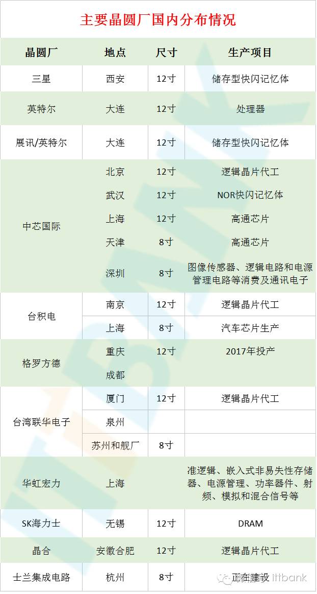
Packaging and Testing Companies:
1. ASE (acquired Siliconware Precision Industries)
2. Amkor (acquired J-devices)
3. Jiangsu Changjiang Electronics Technology (acquired Xinke Jinpeng)
4. Powertech Technology (acquired Chao Feng)
5. UTAC
6. Nanmao Technology
7. Chipbond Technology
8. Tianshui Huada Technology
9. NTC
10. King Yuan Electronics
11. Nepes
12. Unisem
13. Foma Technology
14. Lingsheng Precision
15. Shenzhen Silicon Grids
16. Suzhou Jinfang
17. Wuxi Huada Ansheng
18. Jiasen Semiconductor
19. Wuxi Huajin Semiconductor
20. Suzhou Gude
21. Suzhou Rihua New
22. Shenzhen Baiwei Storage
23. Beijing Shougang Micro (BSMC)
24. Chizhou Huatai Semiconductor (NationT)
25. Qizhong Technology (Suzhou)
26. Ningbo Xinjian Semiconductor
27. Shenzhen Kangmu Technology
28. Jiangsu Xinchao Technology
29. Nantong Huada Microelectronics
30. Freescale Semiconductor (China)
31. Haita Semiconductor (Wuxi)
32. Intel Products (Chengdu)
33. Shanghai Kaihong
34. SanDisk Semiconductor (Shanghai)
35. Qipai Technology
…and many more
ITTBANK (IC Bank):Innovation Achieves Value!

Cloud Egg(ittstore): There is no inventory in this world, just misplaced items!

Global Maker Meeting(ITTChina): Our world changes because of technology!

Welcome to join the ITTBANK QQ group!
Note: Each person is limited to joining one group (if you join multiple groups, you may be rejected, please understand!)!
Welcome to join QQ group (199699487) – Amlogic S802/S805/S812 solution platform network player
Welcome to join AR/VR technology exchange group (527375006)
1. Mobile Industry Technology Exchange Group 3 (134917677)
2. Tablet Technology Exchange Group (378173769)
3. Set-top Box OTT Box Exchange Group (361764225)
4. Capacitive Touch Technology Exchange Group 2 (257209943)
5. Camera Technology Exchange Group (377648136)
6. LCD Screen Technology Exchange Group 2 (249572580)
7. Wireless WIFI Technology Exchange Group 2 (416431905)
8. Security Technology Exchange Group (308535073)
9. Memory Storage Exchange Group (204191613)
10. Mobile, MID, Capacitive Touch, LCD Screen Trading Group (374763457) – Exclusive sales trading procurement group
11. Cross-border E-commerce Exchange (384299409)
12. Global Maker Space (188561451)
13. Dashcam (294132591) – The most professional dashcam evaluation group
14. Global Electronics Technology Exchange Platform (370733047) – (This group is purely a technical exchange group, exclusively for technical engineers, traders please do not enter! Thank you! When adding a group, please add a standard note, region + industry + nickname, e.g., Shenzhen – Bluetooth WiFi Solution – Xie Engineer!)
Submission Email: [email protected]
ITTBANK Customer Service Hotline:
400-0933-666

Click “Read the Original” to enter the ITTBANK WeChat Mall