In high-speed circuit design, we often hear a term—impedance matching. Especially in high-layer PCB designs, impedance control is almost an unavoidable topic. So, why is impedance matching necessary for high-layer PCBs? Today, we will discuss this “invisible killer” that engineers are concerned about.
🚀 Why is Impedance Matching Important?
In low-speed signal circuits, wires behave more like a “conductive copper wire,” with current flowing from one end to the other without much consideration.
However, as signal speeds increase (higher frequency, steeper edges), PCB traces no longer act as “copper wires” but transform intotransmission lines.
On transmission lines, signals propagate in the form of electromagnetic waves, and at this point, the traces have a fixed characteristic impedance. If the impedances between the signal source, traces, and load are inconsistent, it will causesignal reflections, leading to waveform distortion, timing errors, and even complete system failure.
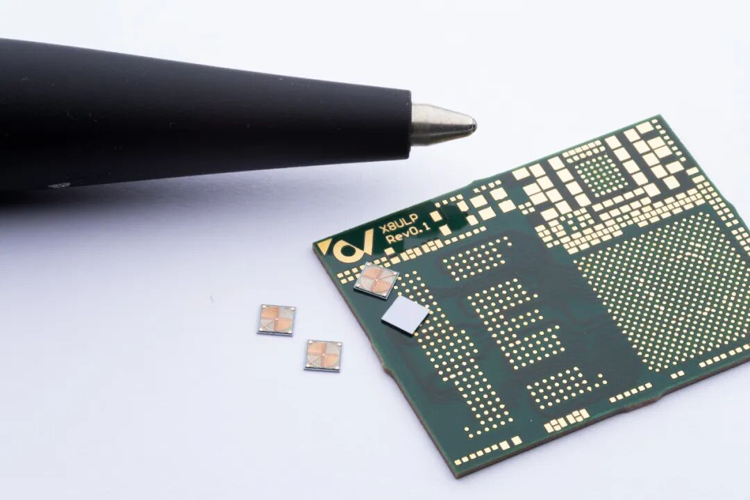
For example, if a high-frequency trace uses 1oz thick copper with a width of 0.5mm, it will alter the inductance, capacitance, and resistance along the trace. This poses challenges for high-frequency signal lines, as capacitance and inductance can change the signal frequency, resulting in completely different outcomes at the start and end of the trace, leading to significant signal attenuation.
Now, let’s look at the following diagram:
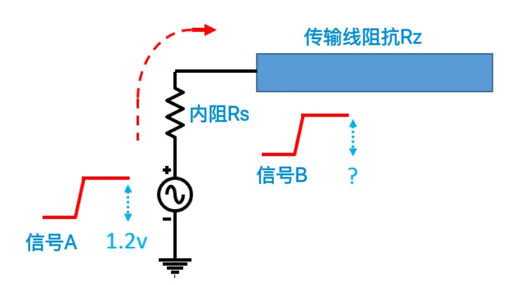
Assuming the internal resistance Rs of the signal is 48 ohms, and the internal resistance of the transmission line is 40 ohms, the amplitude of signal A is 1.2V, then the amplitude at point B after the transmission line would be 545mV; if the driving capability of signal A is stronger, reducing the internal resistance to 34 ohms, then the amplitude at point B would be 649mV.
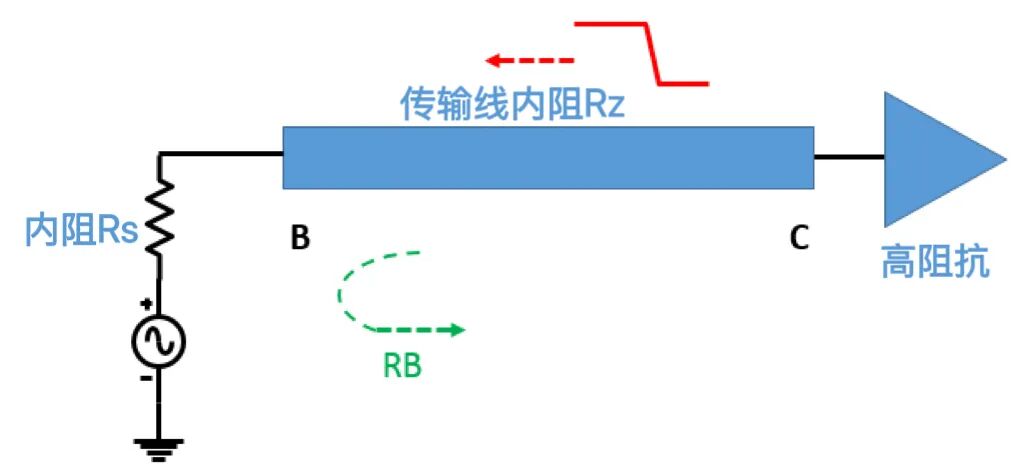
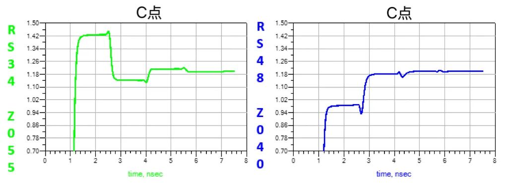
If there is a high impedance line behind the transmission line, the signal at point C will be reflected.
As you can see, the internal resistance Rs and the impedance of the transmission line both affect the terminal signal, which can lead to insufficient driving signal capability or overshoot, causing various signals in the same group to arrive at their destination at different times, degrading timing and resulting in signal chaos or slower speeds.
In simple terms:
- Good impedance matching → Smooth signal transmission, clear eye diagram, reliable system;
- Impedance mismatch → Reflections, crosstalk, overshoot, undershoot, a host of problems await you.
Therefore, to ensure that the carefully designed signal traces maintain signal quality without degradation, we need to carefully control different impedances in various locations.
📐 The Significance of Impedance Matching in High-Layer PCBs
One important role of high-layer boards is to providea reasonable routing environment for high-speed signals. Common practices include:
- Placing a complete ground or power plane directly beneath the signal layer;
- Controlling trace width, dielectric thickness, and dielectric constant to form stable characteristic impedance;
- Allowing signals to propagate along defined paths to reduce EMI and crosstalk.
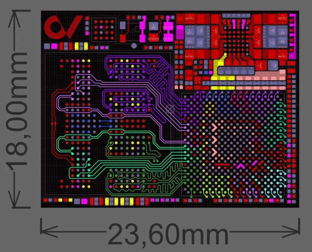
Thus, in high-layer designs, impedance matching is not only a guarantee of signal integrity (SI) but also a key factor in whether the entire board can power up successfully at once.
🔧 Common Impedance Matching Methods in Engineering
- Termination Resistor Matching: The most common method, such as placing termination resistors on DDR, LVDS, and USB differential lines.
- Differential Impedance Control: Designing differential line width and spacing to ensure 100Ω or 90Ω differential impedance.
- Layer Stack Design: Controlling dielectric thickness and line width in the stack according to design requirements (e.g., 50Ω single-ended impedance).
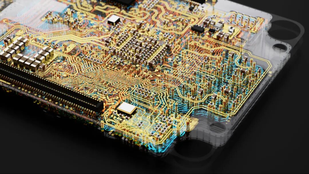
Common PCB impedance requirements for interfaces:
| Signal Type/Interface | Impedance Requirement | Common Notes |
|---|---|---|
| Single-ended Signals (e.g., Clock Lines, Control Lines) | 50 Ω | The standard most common single-ended impedance, almost all high-speed single-ended signals require 50Ω. |
| USB 2.0 (D+/D-) | Differential 90 Ω | USB 2.0 full-speed/high-speed requires differential 90Ω; usually no strict termination resistors are needed. |
| USB 3.x (SuperSpeed) | Differential 90 Ω | Stricter requirements for impedance consistency and trace length, with greater impact from vias. |
| HDMI | Differential 100 Ω | TMDS differential pairs, impedance must be strictly controlled, otherwise image interference may occur. |
| LVDS | Differential 100 Ω | Commonly used in display interfaces (LCD, cameras), low-voltage differential signals. |
| PCIe | Differential 85 Ω | All generations (Gen1~Gen5) require differential 85Ω, with trace symmetry being critical. |
| SATA | Differential 100 Ω | High-speed storage interface, differential impedance must be precise. |
| DDR1/2/3/4/5 Data Lines | Single-ended 50 Ω | Data lines DQ, clock CK, command/address lines all require single-ended 50Ω. |
| DDR1/2/3/4/5 Differential Clock | Differential 100 Ω | DDR CK/CK# differential pairs. |
| Ethernet (100M/1000M/10G) | Differential 100 Ω | Common RJ45 gigabit network ports are all differential 100Ω. |
| MIPI DSI/CSI | Differential 100 Ω | Mobile high-speed interfaces, with strict requirements for trace length matching. |
| Thunderbolt/Type-C High-Speed Lines | Differential 85 Ω / 90 Ω | Similar to PCIe/USB3, usually 85Ω. |
In summary: Impedance matching cannot be solved merely by “drawing good traces”; it is the result of comprehensive optimization of stacking, routing, and simulation.
⚡ Case Study
A certain development board uses DDR3 SDRAM, operating at a rate of 800Mbps. The main control chip is connected to the memory chip via traces, including clock lines, command/address lines, and data lines.
In the first design, the engineer simply followed conventional wiring without strictly controlling impedance:
-
The actual impedance of the data lines (DQ) fluctuated between 40Ω and 60Ω;
-
The differential clock line impedance was close to 120Ω (designed too wide).
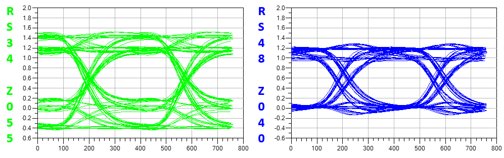
As a result:
After powering on, the system occasionally worked, but most of the time it crashed. Oscilloscope waveforms showed significant reflections and overshoot in the clock signal, and the data eye diagram was severely closed.
The engineer optimized the PCB for impedance matching:
-
Layer adjustment: Reduced the thickness of the reference plane dielectric beneath the signal layer to maintain the data line impedance at 50Ω ±10%.
-
Differential pair optimization: Recalculated line width and spacing to control DDR CK/CK# differential impedance at 100Ω ±10%.
-
Termination resistors: Added a 33Ω series resistor at the main control output to suppress overshoot.
After modifying the PCB and re-sampling, the DDR3 system powered up successfully on the first try, waveform tests were normal, the eye diagram was clear, and the system operated stably at 800Mbps;
Reflection issues completely disappeared.
🌟 Impedance Matching Tools
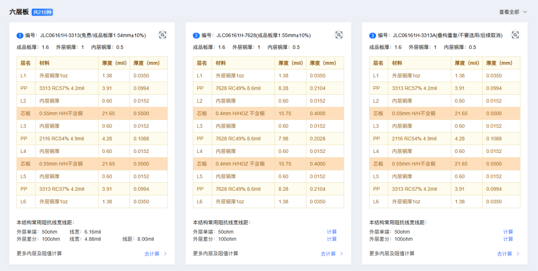
Impedance matching is not only a consideration during the design phase, but the manufacturing process is also crucial. To achieve precise impedance control, high-quality PCB manufacturing is essential. We generally prototype PCBs at JLCPCB, which also offers many useful PCB tools, such as impedance calculation:
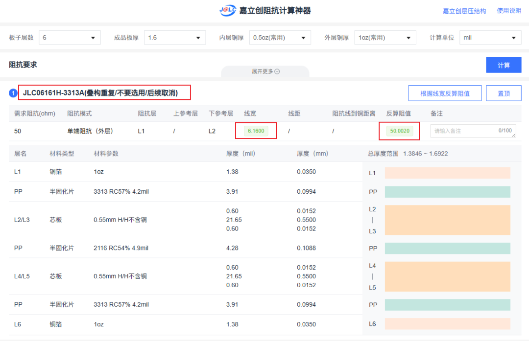
Here, there are many commonly usedlamination structures. After selecting our own lamination structure, the corresponding line widths for common impedances are displayed.
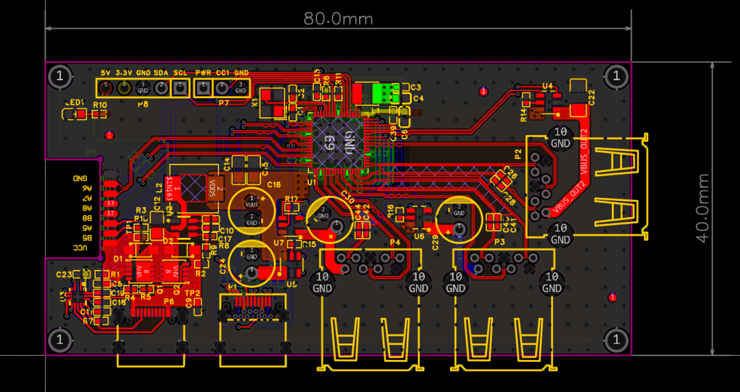
The recently open-sourced 100W PD HUB project by Lao Yu requires impedance matching for USB signal routing, with a differential impedance of 90Ω, usingthe JLC04162H-3313 lamination structure, which offers free impedance control.

In summary, it is very convenient. It helps engineers avoid these “accidents” when placing orders. The boards produced this way not only have a high yield but also ensure signal integrity.
Especially now, with the free upgrade of the gold immersion thickness to 2u for high-quality multilayer boards of 6-32 layers, it is simply delightful.

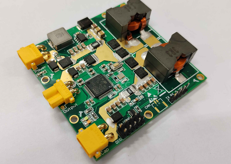 The physical effect is very beautiful
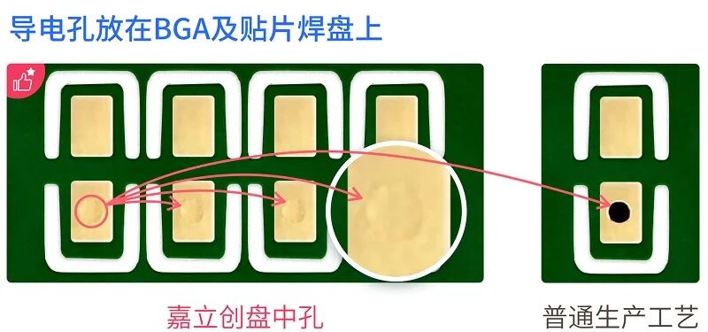
Moreover, with the free via-in-pad process, holes are directly drilled on the pads. PCB with via-in-pad technology outperforms traditional via cover oil and plug oil in both aesthetics and performance. Additionally, using via-in-pad design can significantly save design time and improve product quality.
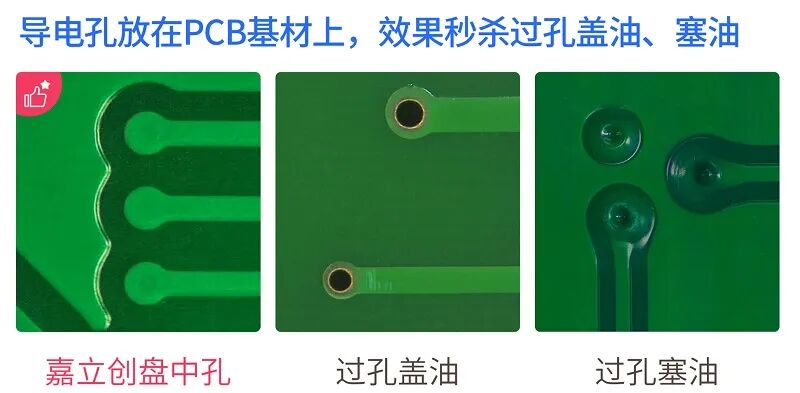
For those who haven’t experienced it, I sincerely recommend you to give it a try!
✨ Conclusion
Impedance matching is necessary for high-layer PCBs because, in high-speed signal transmission, traces have become transmission lines, and impedance mismatch can lead to severe signal quality issues. Through reasonable stacking design and strict impedance control, the reliability of the system can be significantly improved.
So, the next time someone asks you, “Is impedance matching just a gimmick?” you can confidently say: No! It is the soul of high-layer PCBs.
👨💻 Fellow engineers, have you encountered any “pitfalls due to impedance mismatch” while designing high-speed boards? Feel free to share in the comments!