
After familiarizing ourselves with the JTAG architecture through a series of previous articles, let’s take a complete example to understand how the TAP used for Debug access works.
Assuming a debugging scenario where we need JTAG to access and modify a 3-bit wide control signal due to debugging requirements. In normal functional mode, the value of this control signal is 3’b111; however, for some debugging purposes, we want to change it to 3’b100. Below is the process to achieve this through TAP.
Let’s assume the JTAG instruction register (IR) in the design has a width of 4 bits.
First, we need to add a 3-bit wide user data register (User DR) in the JTAG design and connect its output to the control signal we want to modify. Next, we assign an opcode to this User DR, for example, 4’b1010 (since IR is 4 bits, the opcode is also 4 bits). When adding this User DR in the design, we need to set its reset value to 3’b111 (Why? The reset value corresponds to the value needed for this control signal in functional mode, which is 3’b111).
In this way, the User DR will drive this signal to 3’b111 before any JTAG Update event changes its value. Generally, during the chip power-up process, JTAG will exit the reset state earlier than other logic, ensuring that this control signal maintains the desired value of 3’b111 before the logic it drives exits the reset state.
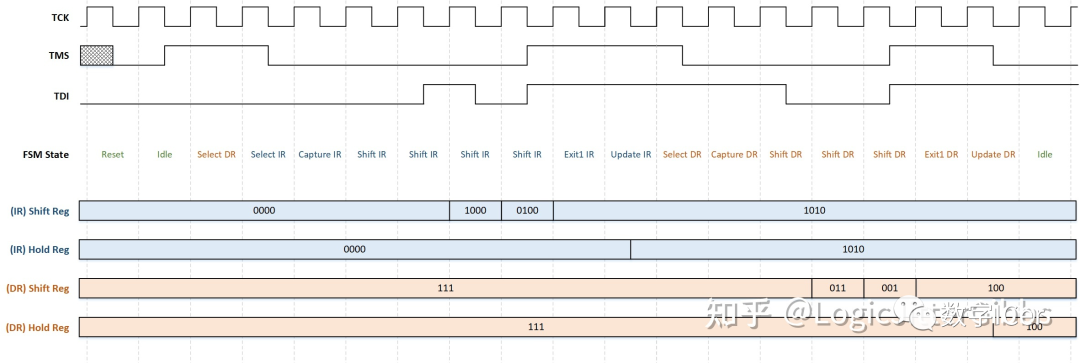
The timing diagram in Figure 1 shows how to update the value of the User DR to 3’b100. This timing diagram comes from the JTAG industrial standard, where TMS and TDI, as well as the IR/DR Hold Register, update their values on the falling edge of the clock, while the FSM state and IR/DR Hold Register change values on the rising edge of the clock.
The 16-state FSM in Figure 1 starts from the Test-Logic Reset state and enters the Shift IR state by setting the timing of TMS.
Next, the corresponding opcode (4’b1010) is shifted into the instruction register via the TDI port. The initial values of the shift and hold registers are both reset values 0, and 4’b1010 is serially shifted into the instruction register from LSB to MSB.
By setting the timing of TMS, the state machine enters the Update IR state. In the Update IR state, the hold register of IR is updated with the value from the Shift register, and the instruction decoder decodes the value of the instruction, establishing a path between TDI and the user data register.
Next, the FSM exits the Update IR state and transitions to the Shift DR state, where the desired value 3’b100 is serially shifted into the DR shift register, from LSB to MSB. Once the data 3’b100 is fully loaded into the Shift register, the FSM jumps to the Update DR state. In this state, the DR hold register is updated to 3’b100, and at this moment, the value of the control signal that needs to be modified also changes from the reset value 3’b111 to 3’b100.
Translated by: Zhihu LogicJitterGibbs Original link: https://link.zhihu.com/?target=https%3A//vlsitutorials.com/jtag-architecture-overview/

Previous Recommendations
SoC Design Bus Interface
SoC Design Low Power
Application of Perl in IC
EDA Tutorial
Chip Design
UVM Chip Verification
FPGA Series
Vivado Advanced
Formal Verification
Digital C Written Test
Digital IC Interview Experience
Excellent IC/FPGA Open Source Projects
Synthesis and Timing Analysis
Statement: Unauthorized reproduction is prohibited