All-Q
2025.11
Paper News
NEWS
This research was jointly completed by the German Electron Synchrotron (DESY) and the University of Hamburg, with core members including Alexander E. Ulanov (experimental design and data processing), Tobias Herr (project guidance), etc. The team has long focused on integrated nonlinear photonics and quantum light source research, achieving a series of results in fields such as micro-combs, slow light, and optical parametric oscillators (e.g., the synthetic reflective self-injection locked micro-comb reported by Ulanov et al. in Nature Photonics in 2024).
====Introduction====
Compressed light is a core resource for emerging quantum technologies such as quantum metrology and quantum information processing, and its efficient generation is a key challenge in the field. Traditional bulk optical systems have achieved high compression levels but lack scalability; while chip-integrated photonic solutions hold promise for solving scalability issues, they are limited by parasitic nonlinear processes (such as single-pump spontaneous four-wave mixing and Bragg scattering four-wave mixing) and significant degradation of compression performance due to optical loss. Therefore, developing an integrated compression light source that combines efficient compression, suppression of parasitic processes, and scalable manufacturing characteristics has become an urgent need in the field of quantum photonics.
Currently, the paths for generating compressed light can be divided into two categories:
- Bulk Optical Systems: Although they have achieved high compression of 15 dB (e.g., periodically poled KTP crystal cavities), they are large, difficult to integrate, and cannot meet the scalability requirements of quantum technology;
- Chip-Integrated Systems: Based on χ⁽²⁾ materials (such as thin-film lithium niobate) for spontaneous parametric down-conversion or χ⁽³⁾ materials (such as silicon nitride) for four-wave mixing, they have scalability but face two core challenges:
- Parasitic Nonlinear Interference: In χ⁽³⁾ systems, dual-pump spontaneous four-wave mixing (DP-SFWM) is accompanied by single-pump spontaneous four-wave mixing (SP-SFWM) and Bragg scattering four-wave mixing (BS-FWM), which inject additional noise into the signal mode, severely weakening the compression level;
- Optical Loss Sensitivity: Compressed states are extremely sensitive to loss; even an additional loss of 0.1 dB can lead to significant degradation of the compressed signal, while the inherent losses of integrated micro-resonators (such as scattering and absorption) and coupling losses are difficult to control.
Therefore, developing an integrated compression light source with “low loss + suppression of parasitic processes + scalability” is a key bottleneck in advancing quantum photonics from the laboratory to application.
2. Core Method: Technical Details from Structural Design to Experimental Implementation
The research team focused onsilicon nitride (Si₃N₄) photonic crystal ring micro-resonators (PhCR) to construct a complete system for generating and controlling compressed light, with technical innovations reflected in three aspects:
(1) Topological Structure Design of PhCR: Static Suppression of Parasitic Processes
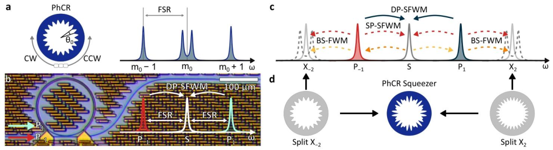
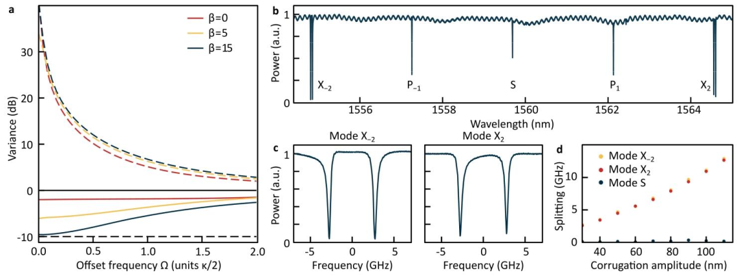
- Customized Nano-Ripples: Periodic nano-ripples are designed on the inner sidewall of the PhCR, with an angular period θ₀=π/m₀ (m₀ is the azimuthal mode order), and the ripples consist of two Fourier components (Figure 1a, d). This structure can accurately couple backward propagating waves (forward CW / backward CCW), causing the target mode X±2 to produce a frequency shift splitting of 5.4 GHz (β≈13.5, β=2γ/κ, γ is the coupling rate, κ is the total loss rate), while the signal mode S (the mode where the compressed light resides) remains unaffected (Figure 2c).
- Physical Mechanism: SP-SFWM and BS-FWM require specific resonant mode matching; the splitting of X±2 causes these parasitic processes to lose resonance conditions, fundamentally suppressing noise injection, and this control is “static”—no thermal or electrical tuning is required, avoiding interference from environmental temperature fluctuations (traditional coupled micro-resonators require dual-cavity thermal tuning, which has poor stability).
- Low Loss and High Q Design: The micro-resonator radius is approximately 75 μm, with a free spectral range (FSR) of 300 GHz, and a waveguide cross-section of 1.6×0.8 μm², achieving anomalous group velocity dispersion D₂/(2π)≈10 MHz; fabricated using commercial foundry UV lithography, the inherent loss rate κ₀≈2π・55 MHz corresponds to a loaded quality factor Q₀≈3.5 million (at a wavelength of 1559 nm), with external coupling efficiency η≈0.9 (which can be increased to 0.95 using a pulley coupler), laying the foundation for low-loss compressed light output.
(2) Physical Mechanism of Compressed Light Generation: Optimization of DP-SFWM
Usingdegenerate dual-pump spontaneous four-wave mixing (Figure 1b, c): Two symmetrically distributed pump lights (P±1) couple into the PhCR, and under the action of parametric gain, the signal mode S (located between the two pumps) generates single-mode squeezed vacuum (SMSV). Key control strategies include:
- Pump Detuning Compensation: Self-phase modulation (SPM) and cross-phase modulation (XPM) can cause pump frequency shifts; by slightly detuning the pump laser from the resonance blue side (thermally locked for stability), this shift can be compensated in real-time;
- Threshold Control: Operating below the optical parametric oscillation (OPO) threshold (approximately 40 mW in experiments, with a working power of 33 mW) ensures the generation of pure squeezed vacuum rather than laser oscillation.
(3) Experimental Setup and Detection Scheme: Precise Quantification of Compression Levels
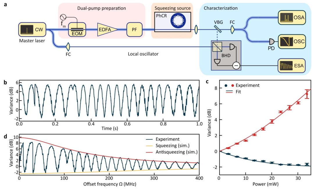
The experimental system is divided into three parts (Figure 3a):
- Dual-Pump Preparation: A single tunable continuous wave (CW) main laser generates dual pumps through an electro-optic modulator (EOM), which are amplified by an erbium-doped fiber amplifier (EDFA) and filtered by a programmable filter (PF) to ensure equal power for both pumps;
- Compressed Light Generation: The pump light is coupled into the chip through lens fibers, and the output light from the PhCR is filtered by a volume Bragg grating (VBG)—reflecting compressed light and transmitting residual pump;
- Balanced Homodyne Detection (BHD): The compressed light is superimposed with a local oscillator (LO, sourced from the main laser to ensure coherence) before entering the BHD, and the output signal is analyzed by an electronic spectrum analyzer (ESA).
- Loss Calibration: Total efficiency T≈0.4 is calculated by independently measuring the efficiency of each stage (Table 1)—external coupling (0.9), chip output (0.94), mode matching (0.81), BHD efficiency (0.75), etc., which is consistent with T≈0.37 derived from the compression/recompression levels, ensuring the credibility of the results.
3. Key Results
(1) Numerical Simulation: Revealing the Impact of Splitting Parameters
Through coupled mode equation simulations of the compression spectrum (Figure 2a), the core conclusions are:
- The anti-compression level remains nearly constant at different β (X±2 splitting parameters), while the compression level significantly increases with larger β—when β≥15, the compression level approaches the theoretical limit corresponding to η=0.9 (10 dB) at low detuning frequencies;
- Physical Essence: The larger the β, the more significant the X±2 splitting, the smaller the noise contribution from SP-SFWM and BS-FWM, and the closer the compression level is to the ideal value.
(2) Experimental Results: Quantifying Compression Performance and Stability
- Static Compression Level: At a 20 MHz sideband frequency, direct measurements show compression of 1.71 dB and anti-compression of 5.54 dB; after loss calibration, the compression inside the cavity is 11.3±0.7 dB, and the total bus waveguide compression is 7.8±1.1 dB (90% confidence interval);
- Compression Spectrum Characteristics: At low detuning frequencies (e.g., 0 MHz), compression is 2.4 dB and anti-compression is 8.3 dB; at 400 MHz, compression is 0.85 dB and anti-compression is 1.3 dB, with the spectral shape highly consistent with the theoretical model (Figure 3d), proving that the compression bandwidth is determined by the cavity linewidth;
- Power Dependence: The compression level increases with pump power until approaching the OPO threshold (Figure 3c), with no significant saturation, indicating that parasitic processes have been effectively suppressed.
4. Scientific Significance and Extensions
- Technical Breakthrough: For the first time, efficient single-mode orthogonal compression has been achieved in PhCR, resolving the contradiction between “suppression of parasitic processes” and “scalability” in integrated compression light sources—static nano-ripples require no active control, compatible with wafer-scale manufacturing, laying the foundation for large-scale quantum chip integration;
- Performance Comparison: The 7.8 dB on-chip compression, while lower than bulk optical systems (15 dB), surpasses existing silicon nitride integrated solutions (e.g., 3.5 dB reported by Shen et al. in 2025), and with optimized waveguide cross-sections (thinner and wider) and improved Q factors, it is expected to exceed 10 dB;
- Application Scenarios: Providing core light sources for quantum-enhanced interferometry (e.g., sensitivity enhancement in gravitational wave detection), Gaussian boson sampling (demonstrating quantum computational advantage), coherent Ising machines (combinatorial optimization), and universal continuous-variable quantum computing, promoting these technologies from “principle verification” to “practical integration.”
——Click the bottom to read the original text directly to the paper homepage———-
Previous Content:
PT Symmetry Achieving Configurable Photon Lifetimes in Quantum Light Sources: From USTC, Huazhong University of Science and Technology, University of Electronic Science and Technology, Shanghai Institute of Microsystem and Information Technology, etc.
MIT Dirk Englund Team: Piezoelectric Driven Silicon Nitride High-Speed Spatial Light Modulator, Speed Greater than 100MHz
Nature Subjournal: Silicon-Based Monolithic Integrated Electro-Optic Platform Above 100GHz
Nature Physics: Learning Quantum States of Continuous Variable Systems
Nature Photonics: A Large-Scale Reconfigurable Multiplexed Quantum Photonic Network
Generating Polarization Entangled Photon Pairs from Two Interacting Quantum Emitters
Lithium Niobate Phononic Crystal Resonators Achieving GHz Electro-Optical Quantum Control
Harvard Marko Lončar Group Lithium Niobate Photonics | Thin-Film Lithium Niobate Terahertz Differential Field Detector with Bandwidth Reaching 3 THz
END
Disclaimer: All content published by this public account, including but not limited to text, images, charts, logos, identifiers, advertisements, domain names, software, programs, etc., unless otherwise specified, is sourced from the internet or user submissions, and the copyright belongs to the original author or original source. This article has been marked with the source. We are committed to protecting the original author’s copyright; if there are any copyright issues, please contact us in a timely manner for processing.