Traditionally, the CPU microarchitecture is understood in a narrow sense, typically from the perspective of pipelining and superscalar pipelines. ARM’s CPU cores also exhibit such microarchitectures. However, ARM’s greatest success lies in its SoC architecture, which likely stems from its positioning as an “IP supplier.” This positioning allows for a fully decoupled design of various modules involved in SoC, enabling diverse IPs to be selected and combined by various customers. Therefore, when examining ARM’s architecture/microarchitecture, one often sees the CPU Core connected by the prominent AXI4 bus (on-chip bus) along with various controllers (including memory controllers, external memory controllers, various peripheral and IO port controllers).This article first examines the microarchitecture of the ARM CPU Core to further understand pipelining and superscalar pipelines, and then looks at the distinctive microarchitecture of ARM’s SoC.1. Microarchitecture of ARM Cortex-A9 CPU Core.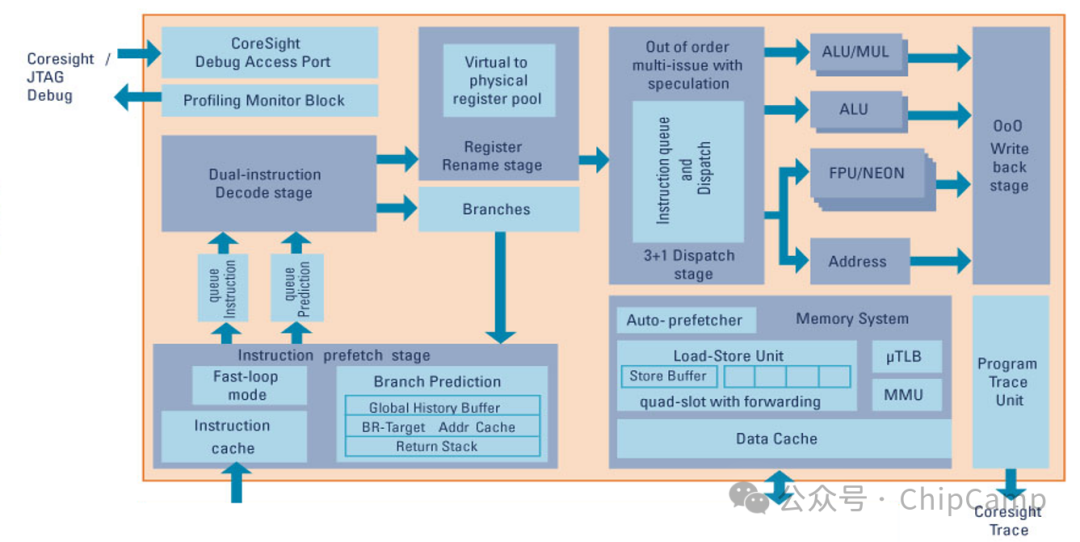 —- Clearly illustrates the pipeline stages: InstrPrefetch, DecodeStage, RenameStage, DispatchStage, WritebackStage.—- The path from InstrPrefetch to DecodeStage consists of two channels! This means fetching 2 instructions at once (via 2 channels), decoding 2 instructions simultaneously, and issuing them. This is the “superscalar pipeline”.—- The instruction fetching part employs branch prediction (including GHB, RAS, etc.).—- After decoding, the design implements a rename mapping, mapping a small number of virtual register files/architectural register files (ARF) to the physical register file (pool) (PRF).—- The instruction issuing after the register stage uses both the terms Issue (issuing) and Dispatch (dispatching), without getting entangled in the distinction between the two. Multi-issue means multiple issuing.—- The memory section includes an MMU, which maps virtual addresses to physical addresses, and the TLB is the page table cache located within the CPU Core.—- The TraceUnit is a debugging point system within the chip, where different levels of software need to construct a trace point system at various levels and between levels, and the CPU Core itself must also have such a debugging and trace point system.2. Microarchitecture of ARM Cortex-A76.
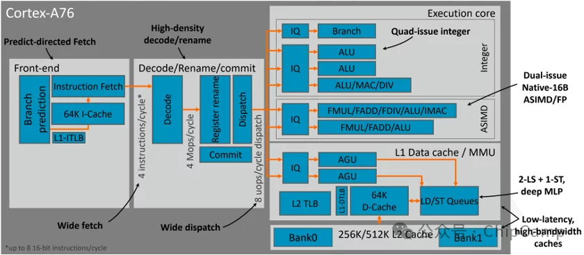 —- The pipeline width from InstrFetch to Decode, and from Decode to Rename is 4, which is double that of the previous example. The wide fetch and wide dispatch in the diagram illustrate the concepts of “multiple issuing” and “superscalar”.3. Microarchitecture of ARM Cortex-A77.
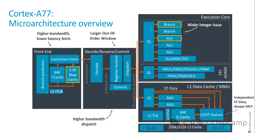 —- The pipeline width has increased again, from 4 instrs/cycle to 6 instrs/cycle.4. A different perspective on the superscalar microarchitecture of ARM Cortex-A9.PipelineMicroarchitecture.
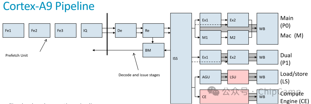 —- From the perspective of the pipeline, there is not much difference between ARM and X86!—- The CPU microarchitecture and ISA instruction set are decoupled; the x86 instruction set has various manufacturers designing and implementing their own microarchitectures, the RISC-V instruction set also has different manufacturers designing and implementing their own microarchitectures, and ARM’s instruction set itself has v5/v6/v7, etc. Based on a certain ARM instruction set, there can also be different microarchitecture designs and implementations, such as whether the pipeline width is designed to be 2 or 4.5. The “abstract” architecture of ARM SoC.
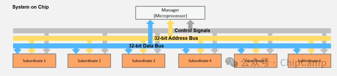 — The bus is the skeleton, and the MicroProcessor is just one of the many nodes hanging on the bus! As a Master/Manager.6. An SoC can integrate multiple CPU Cores, meaning multiple Managers.
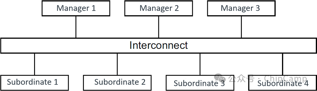 7. An example of a “specific” architecture of an SoC.—- There are 4 CPU Cores, which need to be connected laterally using a high-speed internal bus.—- Not to mention the connections and communications between the CPU and various controllers.
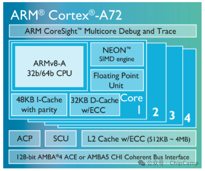 8. A more detailed example of an ARM SoC.
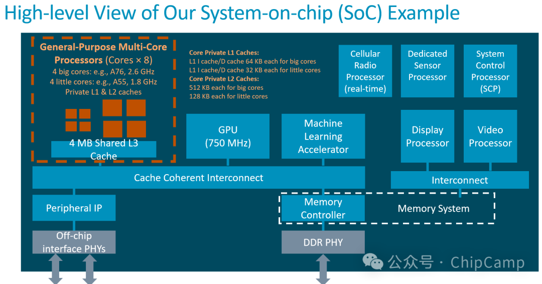 —- A total of 8 CPU Cores, 4 large and 4 small. 1 GPU for graphics processing. 1 machine learning accelerator. 1 Memory Controller. All of these require high-speed interconnects with cache coherence!—- Video processors (connected to cameras) and display processors (connected to displays) use streaming interfaces but are relatively “peripheral” controllers compared to the previous major components.—- The Memory Controller and peripherals are unified in addressing, as indicated by the virtual box in the lower right corner of the diagram.—- This is particularly enlightening, as it shows that the internal memory controller of the chip manages the address space uniformly, and uses a unified memory address bus (e.g., 64bit) and appropriate control signals for management, where the memory read/write commands issued by the CPU and IO read/write are completely consistent Load/Store. The memory controller routes the read/write commands to DDR_PHY or IO_Device based on the address range. The CPU and peripheral controllers are quite decoupled, with the CPU almost not directly perceiving it, but managed through the address partitioning and management by the internal memory controller. Regarding this point, a code example will be referenced at the end of the article for understanding.9. A more specific example of an SoC.
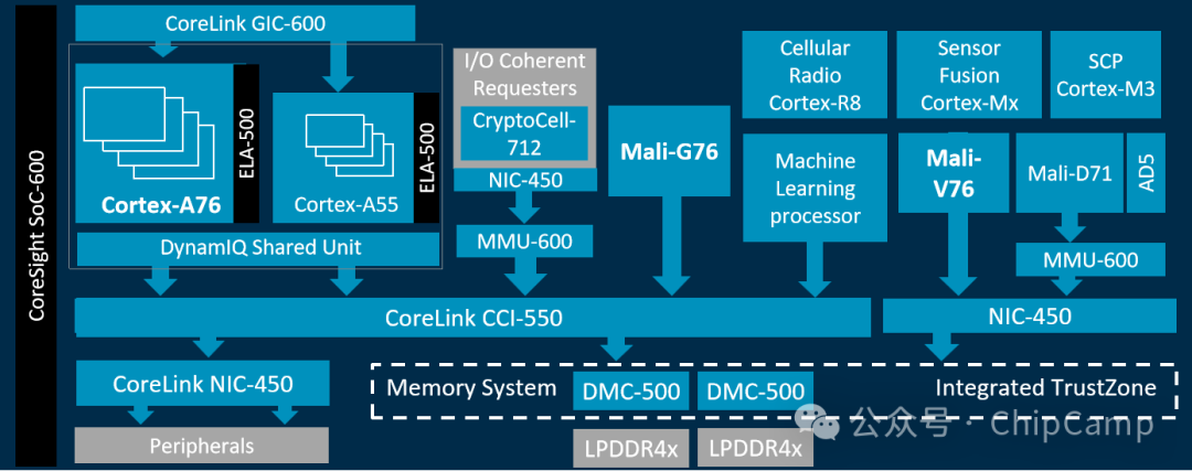 —- The DMC-500 is a DRAM controller, which is an IP unit that ARM can “sell.” This reminds one that MIPS also produces such memory controller IPs. But ARM’s advantage lies in its established CoreLink CCI memory bus specification, which has become part of its product family (IP family)! This includes MMU-600 (which can also be sold separately as an IP), Mali-G76, NIC-450, etc., all based on the CoreLink internal bus. Although there are various external specifications (such as LPDDR4x specifications, NIC’s Eth/Wifi specifications, etc.), the internal bus is a specification that is highly related to product implementation but is highly decoupled. This is why the “on-chip bus” is so important for IP suppliers like ARM.—- The diagram also shows a Cellular Radio Cortex-R8, which is a processor for cellular wireless. This means that ARM SoCs can add significant wireless processing beyond the application processor (from a computing perspective). Clearly, mobile phone SoCs are like this. Wireless signal processing also requires strong processing capabilities (many wireless channels & complex signal processing), especially needing real-time processing!!10. Another example of a Wireless IoT SoC.
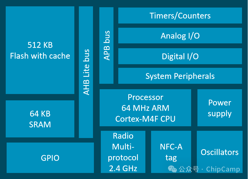 —- The Cortex-M CPU is just a small part. It connects to numerous peripheral devices through AHB Lite and APB buses, including SRAM/Flash and Analog/Radio/NFC controllers, as well as GPIO (the simplest IO that can light up an LED).Appendix 1: Internal memory address partitioning of the SoC Chip, with a specific source code example as follows:
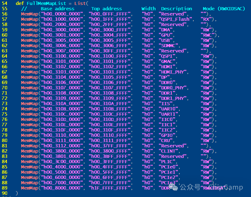 —- DDR0_PHY and DDR1_PHY, like other controllers (such as PCIe, UART, GPIO, etc.), have a register space for peripheral controllers. This space is separate from the DDR memory space itself! The latter occupies the largest address range (5 bits/32 times more).—- Memory (DDR_PHY and DDR), external memory (QSPI_Flash), display, USB, and other familiar interfaces are managed through unified addressing. Additionally, the GPU is also managed through the SoC internal bus and unified addressing, as seen in the actual examples above.Appendix 2: ARM’s first chip and its key figures:
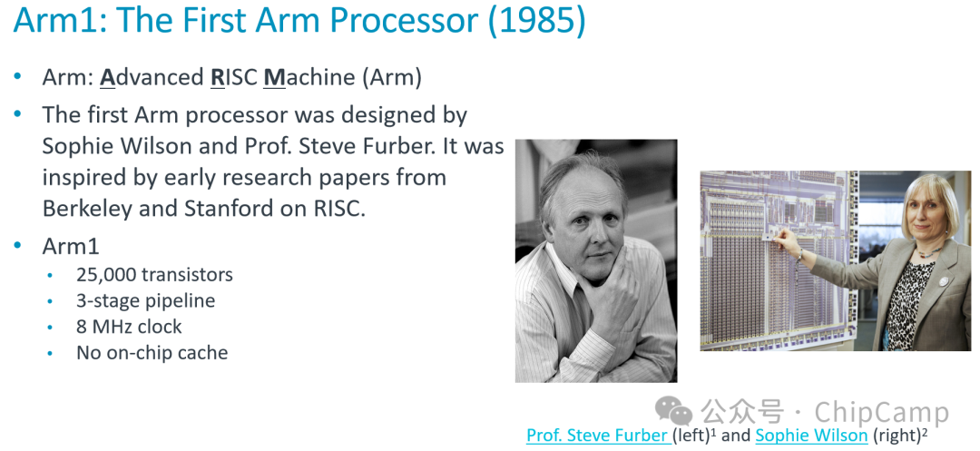 —- Year 1985, figures Steve Furber and Sophie Wilson.—- Designed ARM inspired by RISC from Berkeley and Stanford.—- Berkeley contributed the RISC idea but did not develop MIPS.Stanford’s RISC developed into MIPS. ARM was inspired by RISC, not MIPS.