
Countless nano-sized electronic components are arranged on chips. Are they all pre-manufactured and then placed one by one?
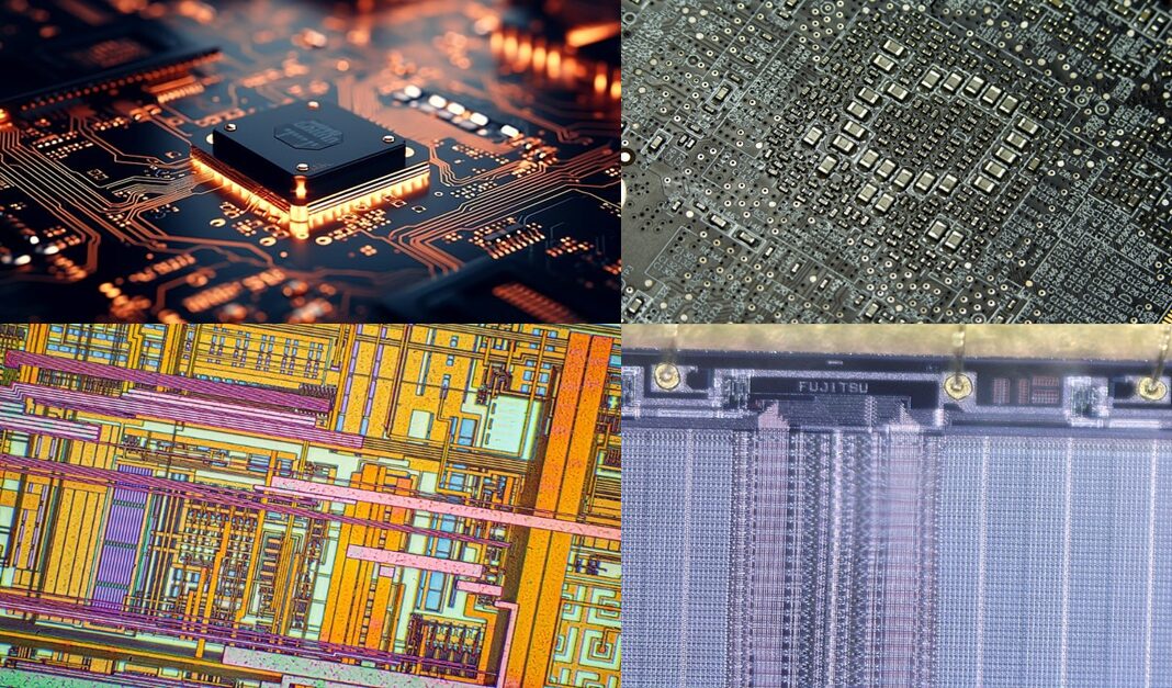
Image source: Pixabay (top); Searchmedia – Wikimedia Commons (bottom)
No! We can look at this issue from a different angle. If we observe vertically, we can see that chips are formed by stacking layers of sheet structures with different patterns. If we pre-manufacture each layer and then stack them vertically, the two-dimensional structures can combine to form a three-dimensional device, ultimately resulting in a chip with rich functionalities.
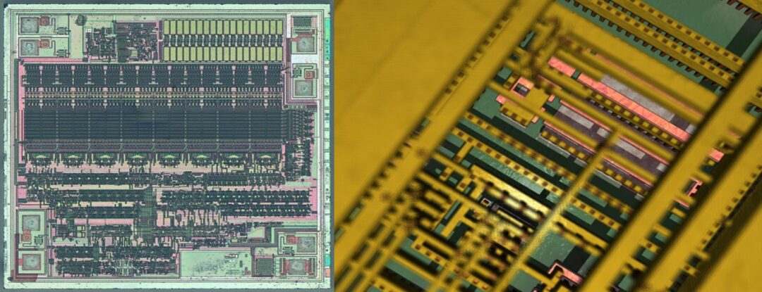
Vertical observation of chip internal structure | Image source: Searchmedia – Wikimedia Commons
Now our goal becomes how to produce sheet structures with specific patterns. First, we need suitable sheet materials to print the circuit diagrams, which is the silicon wafer we often hear about. This is a type of high-purity silicon that is processed and cut into smooth, extremely thin disks.
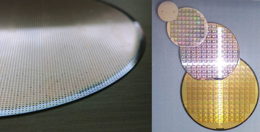
Silicon wafer | Image source: Pixabay (left); Searchmedia – Wikimedia Commons (right)
Next, like carpenters, we need to find the right tools to carve the patterns. To manufacture chips with complex internal structures that are extremely tiny, the size requirements for processing tools are extremely high.
We clever humans found light as our carving tool; because light has a rich spectrum of wavelengths, we can use short-wavelength light to achieve extremely fine processing.
The rich wavelengths of visible light (invisible light has even richer wavelengths) | Image source: Searchmedia – Wikimedia Commons
We hope to transfer the designed circuit patterns onto the silicon wafer through optical exposure, but light cannot affect silicon materials, so we need an intermediate material that can interact directly with light, which is the photoresist.

Photoresist spun onto silicon wafers (evenly covered by centrifugal force) | Image source: Searchmedia – Wikimedia Commons
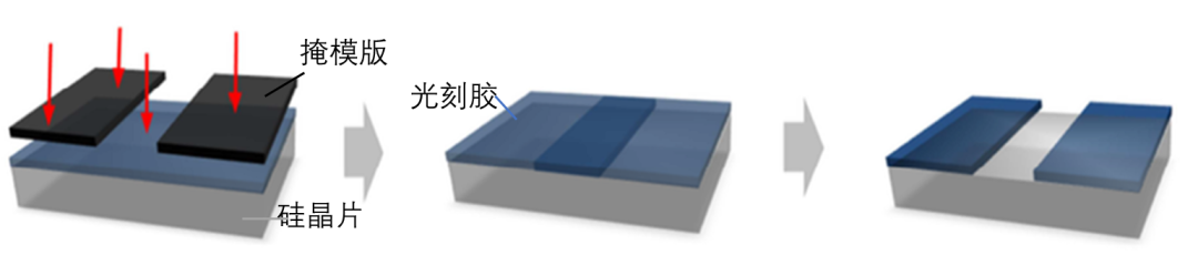
Photoresist imaging exposure process | Image source: Searchmedia – Wikimedia Commons
Photoresist is the main carrier medium for photolithography imaging, divided into positive and negative resists. The area exposed to light that dissolves more easily in the developer is positive photoresist, while the area that is less likely to dissolve in the developer is negative photoresist.
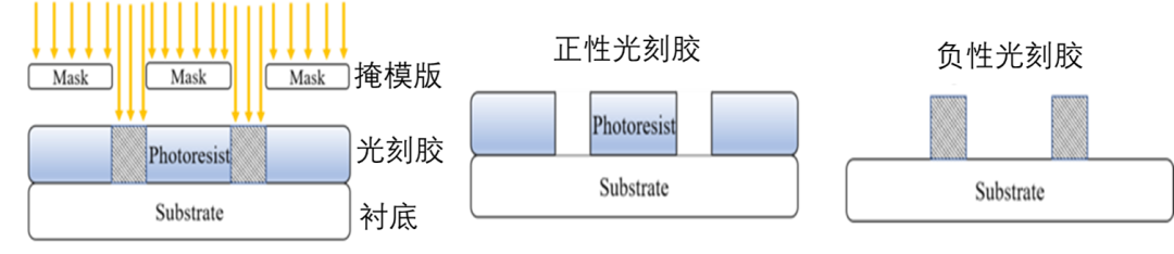
Two results of the exposure process (positive and negative resists) | Image source: Searchmedia – Wikimedia Commons
Assuming positive photoresist is used, after the exposure process is completed, the developer can dissolve the exposed photoresist, and then chemical substances dissolve the exposed silicon wafer, leaving the remaining photoresist on the silicon wafer to protect it. This is the etching process.
Now we have achieved our goal, obtaining a silicon wafer with a specific circuit pattern. Throughout this process, the general idea is relatively smooth, but the precision engineering of chip manufacturing, representing the pinnacle of human wisdom, involves countless stringent requirements.
Applications of Chips
With advanced manufacturing processes, various chips have been born.Some summarize that in the 21st century, chips can be divided into three main categories.
The first type is logic chips, used as processors in our computers, phones, or network servers.
The second type is memory chips, with classic examples including the DRAM chips developed by Intel—before this product was launched, data storage relied on magnetic cores: magnetized components represent 1, and unmagnetized components represent 0. Intel’s approach was to combine transistors and capacitors, where charged represents 1 and uncharged represents 0. Compared to magnetic cores, the principle of the new storage tool is similar, but everything is integrated into the chip, making it smaller and with a lower error rate. Such chips can provide both short-term and long-term memory for computers.
The third type of chip is called “analog chips,” which process analog signals.
Among these chips, logic chips may be more well-known. Although Intel developed the earliest DRAM memory chips, it has been losing ground in competition with Japanese companies. In 1980, Intel reached a collaboration with IBM to manufacture central processing units (CPUs) for personal computers.
With the advent of IBM’s first personal computer, the Intel processor built into this computer became the industry “standard configuration,” just as Microsoft’s Windows system became the more familiar operating system for the masses. This gamble also led Intel to completely withdraw from the DRAM field and rise again.
The development of CPUs was not accomplished overnight. In fact, as early as 1971, Intel produced the first microprocessor (which can only handle a single specific task compared to CPUs), and the entire design process took a full six months. At that time, this microprocessor had only a few thousand components, and the design tools used were only colored pencils and rulers, which seemed as backward as medieval craftsmen. Lynn Conway developed a program that solved the automation design problem of chips. Using this program, students who had never designed chips before could learn how to design functional chips in a short time.
By the late 1980s, Intel developed the 486 processor, capable of fitting 1.2 million micro components onto a tiny silicon chip, generating various 0s and 1s. By 2010, the most advanced microprocessor chips could carry 1 billion transistors. The development of such chips relies on design software developed by a few oligopoly companies.
Another type of logic chip—the Graphics Processing Unit (GPU), commonly known as a graphics card has also gained increasing attention in recent years. In its early days, Nvidia believed that 3D images were the future direction of development, so it designed a GPU capable of processing 3D graphics and developed corresponding software to instruct the chip on how to work. Unlike Intel’s central processing unit, which “calculates in order,” the advantage of a GPU lies in its ability to perform a large number of simple calculations simultaneously.
No one expected that in the era of artificial intelligence, GPUs would gain a new mission. To train artificial intelligence models, scientists need to continuously optimize algorithms using data, allowing the models to complete tasks assigned by humans, such as recognizing cats and dogs, playing chess, or conversing with humans. At this time, GPUs, developed to perform multiple calculations simultaneously for “parallel processing” of data, have unique advantages, and they have also gained a new lease on life in the era of artificial intelligence.
Another important application of chips is communication. Irwin Jacobs saw that chips could handle complex algorithms to encode massive amounts of information, leading him and his friends to establish Qualcomm and venture into the communication field. We know that the earliest mobile phones were also called “brick phones,” resembling a black brick.
Subsequently, communication technology has developed rapidly—2G technology can transmit images and text, 3G technology can open websites, 4G can stream videos smoothly, and 5G offers even greater leaps. Each G here represents a “generation.” We can see that every generation of wireless technology has exponentially increased the information transmitted through radio waves. Nowadays, we feel impatient if there is a slight lag while watching videos on our phones, not realizing that just over a decade ago, we could only send text messages.
Qualcomm participated in the development of mobile technologies from 2G to the later generations. Using chips that evolve according to Moore’s Law, Qualcomm can place more mobile calls into limitless space through infinite frequency. To upgrade to 5G networks, not only do new chips need to be placed in phones, but new hardware also needs to be installed in base stations. These hardware and chips, with more powerful computing capabilities, can transmit data faster wirelessly.

Content source: Popular Science China, Big Data Digest, Unsplash
“Millions of IPs Create Popular Science,” Nationwide Popular Science Carnival is Launched!
Give You a Reason to Sleep Early: Lack of Sleep Will…
A Picture Tells You How Scary Surrogacy Is!