Click the blue textto follow us
Through high selectivity etching, specialized etching tools remove or etch materials from the microchip structures during the IC production process. Furthermore, these high selectivity etching tools can remove materials in any direction (isotropic) without damaging other parts of the device. In some cases, high selectivity etching tools can also remove materials in one direction (anisotropic). Today, some existing etching tools can perform selective etching to a certain extent, but their capabilities are limited, and they cannot create new device structures at advanced nodes.
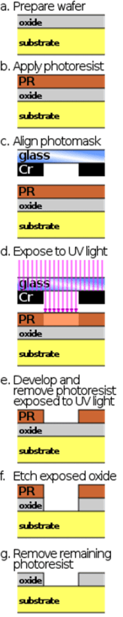
Etching is an essential process in wafer fabrication. In a simple process flow, silicon dioxide material is deposited on the wafer. Then, a photolithography system forms tiny feature patterns on the material of each die on the wafer, and the etching tool removes unwanted material from each die to create various structures, aiming for angstrom-level precision (1Å = 0.1nm).
Essentially, advanced etching tools are standalone systems with a chamber. During operation, the wafer is inserted into the chamber. In one type of etching, plasma (an ionized gas) is generated in the chamber. “First, we create plasma. Electrons collide with gas molecules. This generates ions and more electrons. They also produce free radicals. Free radicals become the substances for chemical etching in the plasma etching system. These free radicals diffuse to the wafer surface. They may react with one material but not with another material.
Not all chip processes require highly selective etching. In chip production, many etching steps are straightforward and utilize existing etching tools. For more demanding chip processes, etching suppliers offer various options involving more complex tools. High selectivity etching is one such option. Using proprietary chemicals, etching tools with these capabilities can remove target materials without modifying or removing surrounding layers.
During the etching process, the etchant (plasma, gas/vapor, acid) bombards the wafer. The etching substance reacts slowly with the mask material but reacts quickly with the exposed silicon dioxide and removes it.
“Selective etching refers to the process of removing materials with an extremely high selectivity of >1000:1, with minimal material loss: <2Å or one single atomic layer. In summary, normal etching selectivity is in the range of 20:1,” said Ian Latchford, Product Marketing Director at Lam Research.
Nevertheless, an increasing number of applications require highly selective etching. All of these require specialized and expensive selective etching tools with complex chemical compositions.
Etching Modes
Technically, selective etching is an application rather than a standalone category. It applies to both wet etching and dry etching categories. In all cases, the goal is to achieve precise etching on the wafer with good uniformity.
Sputtering or ion beam etching is a physical process. During operation, the chip is inserted into the system. The tool generates ions at an accelerated speed, thereby removing materials from the chip.
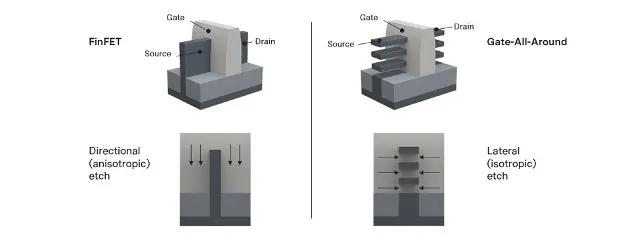
Each etching mode has different properties, such as selectivity and directionality. Directionality involves anisotropic and isotropic etching.
ALE and Selective Etching
In one example of ALE, the wafer is located in the chamber of the ALE system. The first step is to inject chlorine gas onto the silicon surface in the chamber. Chlorine molecules are adsorbed on the surface, altering it. Then, argon ions are injected into the chamber, bombarding the surface and removing the modified layer.
There are two types of ALE—plasma and thermal. Plasma ALE in production can achieve anisotropic etching. Thermal ALE, still in development, uses thermal reactions for isotropic etching.
“Plasma or thermal ALE is more about extreme control of the etching front rather than overall selectivity,” said Bézard from Imec. “Sometimes it is better than traditional plasma etching, and sometimes it is worse. But the selectivity is far below the levels required and achieved by high selectivity etching.”
Additionally, ALE is slow and has limited isotropic capabilities. In some cases, ALE can cause minimal damage to structures.
Regardless of the application, all processes are challenging.
Applications
High selectivity etching has various applications. For example, anisotropic high selectivity etching is used to form self-aligned contacts. In chips, contacts are tiny structures that connect transistors to the first layer of copper interconnects in the device.
Other selective etching processes are used in GAA. At the 3nm and/or 2nm process nodes, leading foundries and their customers will ultimately migrate to a type of GAA transistor called nanosheet FET. Nanosheet FET is a finFET rotated 90 degrees, forming horizontally stacked fins with vertical gate material between each fin. Each fin is like a sheet of paper, serving as a channel.
Conclusion
High selectivity etching is an important complement to the toolset. “These solutions enable chip manufacturers to produce increasingly powerful and complex chips that can support compute- and performance-intensive technologies such as autonomous vehicles, advanced digital healthcare, and the upcoming metaverse.

Wuxi Qixin Semiconductor Technology Co., Ltd. is a high-tech enterprise specializing in the R&D, production, and sales of intelligent production equipment for the chip industry. Established in 2020, it is located in the Wuxi Huishan Economic and Technological Development Zone. The company has received multiple honors, including Pioneer Talent in Wuxi Huishan District and Taihu Talent in Wuxi City, and is a council member of the Wuxi Semiconductor Association. The core members of the company’s R&D team have over 20 years of experience in semiconductor equipment, with rich R&D experience in packaging processes and related equipment industrialization, holding multiple national-level technology invention, utility model patents, and software copyrights. The company has long-term industry-university-research cooperation with well-known domestic institutions such as Tsinghua University and the Chinese Academy of Sciences.
The self-developed MGP intelligent chip packaging system, AM fully automatic chip packaging system, TF unit modular chip automatic cutting and forming system, and other intelligent production equipment for chips have all received market recognition and unanimous praise from customers.
Wuxi Qixin Semiconductor Technology Co., Ltd. adheres to the values of innovation, efficiency, quality, and integrity, based in Wuxi, with the mission of creating intelligent equipment for China’s independent brand chips, supporting the chip industry, and building smart factories. It aims to become a leader in the chip packaging and testing equipment industry!
Disclaimer: This article is a network reprint or adaptation, and the copyright belongs to the original author. However, due to numerous reprints, it is impossible to confirm the true original author, hence the source is indicated. If there are any copyright issues, please contact us for deletion! The content of this article reflects the views of the original author and does not represent the views of this public account or its responsibility for authenticity.