
Introduction
The STM32 provides flexible and diverse access implementations for external memory. This article will introduce how to utilize QSPI (QuadSPI) to implement external serial NOR Flash memory. First, the functional characteristics of the QSPI interface will be introduced, followed by hardware design and software development. Based on STM32CubeM, a reference implementation for accessing the MICRON N25Q128A13EF840F will be provided.
1. Implementation Environment
Development Board: STM32F469G-DISCO
Development Library: STM32CubeF4 v1.16.0
STM32CubeMX: v4.22.0
Integrated Development Environment: IAR v7.70.1.11486
The implementation process is carried out on the STM32F469I-DISCO board, utilizing the onboard serial NOR Flash memory (MICRON N25Q128A13EF840F) to present the entire development process. In this article, the hardware connection between QSPI and external serial memory is introduced based on the QSPI interface. Additionally, the Cube software package includes QSPI instances, but this article does not discuss the implementations within the library; readers can refer to these QSPI examples for design. This article focuses on how to access external serial NOR Flash memory using the project generated by STM32CubeMX.
2. Introduction to QSPI
Before presenting examples of QSPI accessing external Flash, a certain understanding of QSPI is necessary, and a brief introduction will be provided here. For more content, please refer to AN4760.
QSPI (Quad-SPI) supports a four-wire serial access format. At the same time, QSPI supports traditional SPI and Dual-SPI modes, with Dual-SPI mode supporting two-wire serial access. Compared to FMC/FSMC, QSPI supports lower-cost, smaller package external serial Flash memory with fewer IO pin usages, effectively reducing PCB area and lowering PCB design complexity.
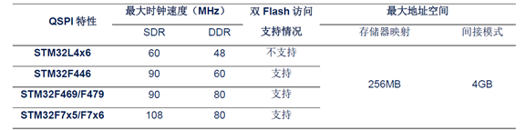
The table below shows the support status of QSPI in different STM32 product lines (only partially listed and not covering all supported models).
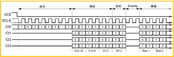
The QSPI interface provides five configurable stages as shown in the figure below (the timing diagram may vary based on configuration). These stages are command phase, address phase, multiplexed byte phase, dummy phase, and data phase. Different stages can be configured based on the command timing in the external Flash. Subsequent examples will be presented. For more content, please refer to AN4760.
QSPI supports three modes:
Indirect Mode → All operations are implemented through QSPI registers, similar to traditional SPI. Blocking mode, interrupt mode, or DMA mode can be used for read and write access. The implementation example provided in this article is for the indirect mode.
Polling Mode → The interface automatically polls a specified register until the read-back register content matches the specified condition. This can be applied to state detection, thus achieving busy-waiting effects. This mode will not be introduced in this article; application implementations can refer to the QSPI examples in the Cube software package.
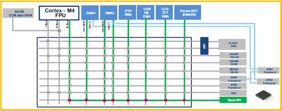
Memory-Mapped Mode → The external Flash is treated as internal memory, supporting direct access by AHB master devices, allowing the CPU to execute code located in QSPI memory directly. The internal system architecture is shown in the figure below (using STM32F469/F479 as an example). This mode will not be introduced in this article; application implementations can refer to the QSPI example QSPI_ExecuteInPlace in the Cube software package.
3. Implementation of QSPI External Serial Flash
3.1 Introduction to Serial Flash
Taking MICRON N25Q128A13EF840F as an example, for more details please refer to the memory manual. The pin diagram, timing diagram, and electrical parameters of N25Q128A13EF840F are sourced from the N25Q128A13 manual.
Supported Protocols: SPI, Dual I/O (corresponding to Dual-SPI), Quad I/O (corresponding to Quad-SPI)
Supported Access Modes: Single-line access, dual-line access, four-line access, benefiting from the flexible configurability of the QSPI interface, all three access modes are supported.
Power Supply Voltage Range: 2.7 ~ 3.6V
Maximum Clock Frequency: 108MHz
Storage Space: 128Mb (16MB)
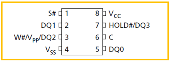
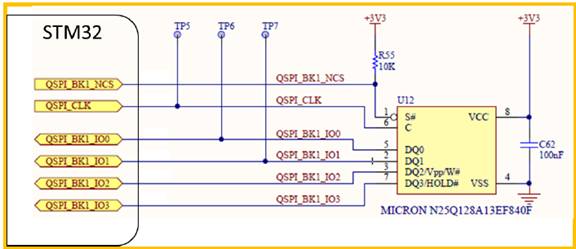
The device pin schematic is shown below, consisting of two power pins and six QSPI signal lines.
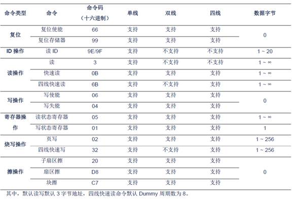
The table below lists the commands for the memory N25Q128A13xxx (not all commands are listed). From this table, it can be seen that the memory provides flexible access implementation forms, combined with the similarly flexible and configurable QSPI interface, enabling full support for memory commands. This article only provides design ideas and presents part of the commands implemented on QSPI.
3.2 Hardware Design
With few signal lines involved, the hardware design is simple; just directly connect the six signal lines of QSPI to the memory. For testability, series resistors or test points can be added. The hardware circuit diagram is shown below.
QSPI interface PCB design follows the following points; for more hardware design content, please refer to AN4488.
a. Line resistance 50Ω± 10%
b. Maximum line length <120mm
c. Avoid routing signal lines on different signal layers
d. The clock line should be at least three times the line width away from other signal lines
e. Data signal line length difference ≤10mm
f. Avoid serpentine routing for clock lines and minimize vias on data lines.
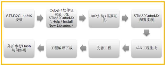
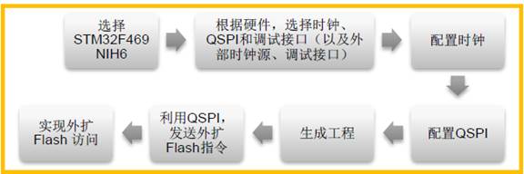
3.3 Software Development Process
3.4 Software Implementation Example
Once the environment is set up, you can use STM32CubeMX to configure QSPI based on hardware connections and obtain the IAR project. The specific software implementation process is as follows.
4. Conclusion
The QuadSPI interface of STM32 is flexible and configurable, allowing configuration for command phase, address phase, multiplexed byte phase, dummy phase, and data phase. Based on this flexibility, support for SPI, Dual IO, and Quad IO serial Flash available on the market can be achieved. For simplification, more features such as interrupt access and DMA access supported by QSPI are not introduced in this article; further implementations can refer to the QSPI examples in the Cube software package provided by ST. Additionally, the command and operation implementations of serial Flash from different manufacturers may vary slightly, and specifics should be based on the Flash documentation used.
Related Documents
AN4760 Quad-SPI (QSPI) interface on STM32 microcontrollers
AN4488 Getting started with STM32F4xxxx MCU hardware development
RM0386 STM32F469xx and STM32F479xx advanced ARM®-based 32-bit MCUs
For more details on QSPI configuration and code interpretation, please click the lower left “Read Original” to download and read.
================================
Previous Topics Links:
1. How to configure CRC parameters in IAR
2. A case of system crash caused by using external SRAM
3. Leakage current analysis in STOP2 mode of STM32L4
4. Demonstration and explanation of IAP functionality using USB DFU
5. Ways and means to obtain ST MCU technical materials and related support