If you have been following the news about 5G, you know that it can significantly increase bandwidth, reaching up to 10Gbps. Additionally, it has a system latency of less than 1ms, with greatly reduced power consumption compared to existing networks. 5G will enable a plethora of new applications in areas such as industrial IoT, vehicle-to-vehicle communication, and edge computing. Beyond high bandwidth and ultra-low latency, these applications also require two other less-discussed characteristics: 99.99% reliability and 24×7 availability. This article discusses the important selection criteria for NOR Flash memory in wireless infrastructure applications.
Technology
To respond to the rapidly changing market standards within a compressed time-to-market, Field Programmable Gate Arrays (FPGA) and System on Chip (SoC) have been widely adopted across various wireless infrastructure applications. FPGAs and SoCs need to be configured at every system boot-up. They can be configured through various types of memory, such as Flash, eMMC, unmanaged NAND, and SD cards. Unlike NAND Flash (managed or unmanaged) and SD cards, NOR Flash memory provides high reliability during initial response and boot-up, with low latency, and can survive in the market for 10 years or more. Moreover, advancements in MirrorBit technology (storing two bits per memory cell) support greater density scaling compared to floating gate technology. Higher density enables NOR Flash products with single-chip 1Gb and higher densities required for 5G wireless infrastructure. Due to these features, NOR Flash memory has been widely used in wireless infrastructure applications to configure FPGAs and SoCs, allowing for quick and reliable boot-up of these devices.
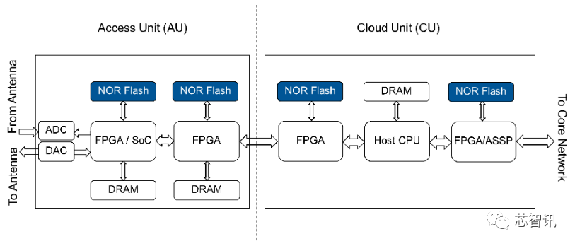
Figure 1: 5G System Schematic. A 64×64 antenna array increases data transmission between the antenna and the digital front end, thereby imposing higher processing requirements on the Access Unit (AU) and Cloud Unit (CU).
Density
5G can utilize frequency bands below 6GHz and at 28GHz. These carrier frequencies are significantly higher than typical 4G LTE frequencies. Although higher carrier frequencies may support more channels as frequency increases, propagation becomes worse. At these frequencies, connections are limited to short-range line-of-sight due to free-space attenuation and the inability of signals to penetrate solids.
As a result, transceivers will have to rely on technologies such as beamforming. Beamforming provides constructive interference to enhance the signal at the receiving end, but cells must be more closely connected.MIMO antennas and their RF front ends are key to implementing 5G access units. For base stations, antennas may be in 64×64 arrays. 64×64 MIMO will explode the front-haul bandwidth requirements (the connection between antennas and digital front ends). Compared to those used in 4G LTE digital units, the FPGAs/SoCs used in access units must have more logic elements (higher density), greater DSP capabilities, and more transceivers. This increase in demand will result in larger configuration images, requiring higher-density single-chip NOR Flash memory for FPGA/SoC configuration. For 5G access units, this density ranges from 512Mb to 2Gb.
Interface
FPGAs and SoCs can be configured/booted using two different types of interfaces (parallel and serial). Although parallel interfaces support faster read/write times, they require too many IOs. For example, consider connecting a 1Gb parallel NOR Flash to an FPGA; the required number of IOs is 49. However, with each increase in density (2G, 4G, 8G, etc.), the number of pins increases by 1.
NOR Flash serial interfaces are based on the common SPI interface on controllers. They use SPI (1-bit), Dual-SPI (2-bit), Quad-SPI or Q-SPI (4-bit), and even Octal-SPI (8-bit) interfaces. Engineers are migrating from parallel to serial interfaces for new system designs. Serial interfaces reduce the pin count for both memory and SoC, shrinking the PCB and thereby lowering costs and form factor. Octal SPI and HyperBus interfaces now offer performance up to 400MB/s, comparable to parallel interfaces. Note that while the recently released Xilinx Versal FPGA supports Octal SPI and Q-SPI interfaces, 14nm and higher-level FPGAs/SoCs only support Q-SPI interfaces.
Voltage
In addition to parallel and serial interfaces, the voltage requirements of the interfaces are also an important selection criterion. Today, FPGAs/SoCs for 5G will be developed with advanced process nodes that reduce 3V voltage I/O support to enhance IC reliability and performance. Most Flash on the market is 3V components (which means they need to operate within a voltage range of 2.7V to 3.6V). However, the latest FPGAs/SoCs require 1.8V NOR Flash components (which need to operate within a voltage range of 1.7V to 2.0V). As FPGAs and other controllers continue to move toward smaller form factors and power supply voltages, 1.2V NOR Flash components are gradually becoming available. While most NOR Flash components require only one supply voltage, 1.2V components require two different supplies. One for the core and the other for IO (input and output high/low conditions referenced to VIO). Separating VIO from VCC provides greater flexibility for system designers but requires additional power supplies.
Almost all 1.2V NOR Flash memory on the market is aimed at consumer applications. Compared to the requirements of 5G wireless infrastructure applications, consumer applications are inherently low-density, making them unsuitable for configuring FPGAs in these applications. Given the available density options and the broad support for 1.8V IO in FPGAs, 1.8V NOR Flash memory remains the most suitable for configuring various FPGAs or booting SoCs for wireless infrastructure applications.
Rated Temperature and Low Power Mode
Wireless infrastructure devices, especially digital front ends such as radios and small cells, are often installed outdoors and face challenges from extreme environmental conditions. Worse still, system designers may have limited ability to install heat sinks and fans on components used in 5G. Therefore, designers typically choose NOR Flash components rated above industrial temperature (-40°C to +105°C) to withstand harsh environmental conditions and provide additional protection in terms of power consumption, ensuring operation and boot-up at these high temperatures.
Deep Sleep and Standby Mode
NOR Flash components are typically idle between FPGA/SoC configuration cycles. Some NOR Flash components feature deep sleep and standby modes that help reduce power consumption by putting the NOR Flash component into low power mode after configuration is complete.
Durability and Data Retention
NOR Flash is optimized for reliability and performance rather than cost (unlike consumer-oriented technologies such as NAND Flash and SD cards). This technology uses relatively large memory cells to provide high durability and long data retention. It is not surprising that products exhibit durability with 100K programming/erase (P/E) cycles and data retention capabilities of up to 10 years. Note that durability is typically not a concern for such applications since Flash can only be written a limited number of times. This is indeed the case if we only consider storing configuration images in Flash. Additionally, some designers also use Flash to cache transactional data and system error logs. In such usage scenarios, system logs may be updated in Flash every few minutes. Therefore, the total number of P/E cycles during an 8 to 10-year lifespan can exceed maximum durability specifications without loss of balance.
New products on the market allow engineers to optimize the balance between durability and data retention by offering durability of up to 1M P/E cycles or 25 years of data retention. These higher reliability products sometimes come with detailed Failure Mode and Effects Analysis (FMEA) to help designers design systems that meet or exceed the ultra-high reliability and availability requirements of 5G specifications. For example, Cypress provides various functional safety documentation, including device safety manuals and detailed safety analysis reports that document product safety architecture and assumptions of use, summarize FIT rates, FMEDA results, complete safety analysis down to the blocking level, safety mechanisms, and diagnostic scope (see NOR Flash for Automotive and Functional Safety).
Security Features
Recently, there was a news report about a long-term massive attack on global telecommunications companies. Security research firm Cybereason reported that attackers leaked call data records during this attack, but they had already taken control of the network and could even shut it down. Due to incidents like these, there is an increasing focus on the protection of wireless infrastructure devices. The simplest way to secure these systems is to protect configuration images/boot code through the deployment of secure boot and access control processes. In response to the growing interest in protecting embedded systems, NOR Flash suppliers have begun developing products with built-in security features, such as public key infrastructure-based authentication and access control, as well as secure boot. These features can add extra measures to ensure the security of proprietary IP, prevent tampering with configuration images/boot code, and ensure continuous network availability.
In storing FPGA configuration images and SoC boot code, NOR Flash is more popular than NAND and SD cards. 5G wireless infrastructure applications require NOR Flash with 1Gb or higher density, 1.8V Q-SPI or Octal SPI, and above industrial temperature to configure or boot the FPGAs and/or SoCs used in the systems. As designers begin to explore 5G wireless infrastructure products, there is increasing attention to fail-safe operations to meet the demands of applications such as electronic health, Industrial IoT (IIoT), and autonomous vehicles. Flash suppliers are now beginning to offer products that provide functional safety and secure boot mechanisms. These features enable designers to offload some of the processing work related to system-level security and safety functions to the memory. Additionally, available accessories help implement these features and shorten time-to-market. Ultimately, choosing the right memory will help ensure the success of the product.
Editor: Chip Smart News – Lin Zi Source: Cypress
Deep dive into advancements in fingerprint/voiceprint/3D face/eye tracking technologies, this biometric technology forum is a must-attend!
IC China 2019: Where are the opportunities in China’s integrated circuit industry?
Wentai Technology’s mid-term revenue of 14.434 billion is expected to exceed 36 billion for the whole year!
AI performance surpasses Snapdragon 855 Plus and Kirin 810! How does Unisoc Tiger T710 achieve this?
OPPO’s “chip-making” prospects?
Size reduced by 50%! With the commercial use of 5G mobile phones, Silicom Micro first launched a new generation CSM optical fingerprint module.
IBM open sources the POWER instruction set, bringing new opportunities for domestic high-performance CPUs?
The nightmare of Arm Mali GPU: Samsung and Huawei turn to self-research!
MIIT’s Wei Le Ping: Domestic 5G investment will reach 1.5 trillion! Where are the opportunities in the component industry?
[In-depth Analysis] The current status and future of brain-computer interface technology!
For industry communication and cooperation, please add WeChat: icsmart01Chip Smart News official communication group: 221807116