
As the demand for faster, cheaper non-volatile memory alternatives continues to grow, especially in applications like automotive, resistive RAM is gaining renewed attention.
Embedded flash memory has long left designers hoping for better write speeds and lower power consumption, but as the technology’s lead shrinks to 28 nanometers, another issue arises. Manufacturing flash memory at these sizes can require dozens of masks, which increases costs. Most importantly, flash memory requires a higher thermal budget and relatively high voltages at the front end.
This is where potential competitors see an opportunity, as they attempt to leverage ReRAM. A key argument from ReRAM advocates is that some new applications require higher performance, and simply scaling up flash to improve speed is no longer feasible.
Traditionally, the memory market, dominated by entrenched players, has been difficult for newcomers and new technologies to penetrate, partly because it is challenging to compete on cost with chip manufacturers that have already fully depreciated their fabs and equipment; partly because existing technologies have proven effective over time; and more importantly, because companies continually innovate to remain competitive in a market with multiple players.
Thus, if these other technologies can establish themselves, they are likely to appear in the high-end segment of the NOR flash market, where new opportunities and higher average selling prices exist, rather than in the mainstream market where NOR may still be viable.
This is especially true in many automotive applications, where cost is a critical factor. “A typical car has about 20 flash devices,” said Jackson Huang, Vice President of Marketing at Winbond Electronics. “There are 6 to 8 cameras in a car with flash. The dashboard uses flash memory, as does the infotainment system. The MCU has a certain amount of flash built in. But what really drives this market is that over the past few years, with the emergence of over-the-air images, the usage of flash has increased significantly in both density and unit shipments. Typically, there are at least 2 images, often 3. You have a default image in case of issues, and you have the current running image, as well as previous images.”
Xi-Wei Lin, Director of Application Engineering for Synopsys’ EDA team, also sees a future with multiple options. “ReRAM can serve as embedded memory for IoT devices or as a standalone unit in MCUs,” he said. “ReRAM is not affected by magnetic attacks, so it may be useful for applications in special environments or with unique security needs. NVM will continue to be application-specific, depending on performance, power consumption, reliability, density, form factor, and cost. In my view, trade-offs are always necessary, and there is no one-size-fits-all solution.”
Market research also supports these conclusions.
According to Business Market Insights, the NOR market is projected to grow at a compound annual growth rate of 14%, reaching $1.64 billion by 2028. Meanwhile, according to Data Bridge Market Research, the value of ReRAM is expected to surpass NOR in the coming years, with a compound annual growth rate of 17.2%, projected to reach $2.16 billion by 2030. Companies remain optimistic about all these memories, especially considering heterogeneous integration and the rapidly growing data volume.
Jack Guedj, CEO of Numen, stated, “Next-generation persistent memories have many advantages over traditional NOR flash, but they have lower durability and poorer write performance.” “For some applications, read performance is also too slow, and active read power is too high. This means SoC designers either read/write directly from these memories or add large SRAM memories to buffer resistive RAM, incurring heavy costs in performance and power consumption.”
ReRAM suffered setbacks after HP abandoned its efforts but has matured in recent years. Established companies and startups have addressed the tricky materials science issues necessary to produce consistent results, and in academic and corporate research labs, ReRAM has become the preferred memory for neuromorphic AI applications, as evidenced by the NeuRRAM chip created in academia last year.
Tony Kenyon, Professor at University College London and CTO of ReRAM startup Intrinsic, reflected on the efforts made to tackle fundamental challenges like stability. “Many papers have been published that can be traced back seven or eight years, where groups were either studying oxides from the periodic table or doping oxides with different elements, trying out some devices, and then moving on to the next one.”
In one of these efforts, IBM chose HfO2-based ReRAM because IBM was already familiar with this material through its pioneering work on hafnium used in logic transistors. IBM is now tuning it to meet the demands of deep learning.
Intrinsic chose to use silicon dioxide. “We can do some more interesting things with oxides,” Kenyon explained. “We can take nominally very insulating materials, very good dielectrics, and by engineering the oxides in a specific way, rather than making defect-free, uniform, flat interface stoichiometric oxides that have been used for decades, we can design the material differently to make it switchable. We can change the resistance between two distinctly different states (high-resistance state and low-resistance state). Depending on how we program and create the device, it can also have more states, in a sense, even simulating changes in resistance, but for memory devices, ReRAM memory devices, two states are a good starting point.”
Basics of ReRAM
While the materials science in ReRAM is extremely complex, the basic theory is relatively simple. ReRAM uses resistance as the basis for switching rather than charge.
“Essentially, it is a resistor with variable resistance that can be changed by applying a specific voltage, and it can be reset and set again,” explained Mark Dickinson, CEO of Intrinsic.
At the core of ReRAM operation are conductive filaments that form and break via two different methods. In OxRAM, a metal oxide material is sandwiched between two electrodes. When a positive voltage is applied to the top electrode, conductive filaments form between the two electrodes. The filaments consist of oxygen vacancies. When a negative voltage is applied to the bottom electrode, the conductive filaments break. Essentially, ReRAM switches between high-resistance and low-resistance states. The change in resistance is represented in memory as “0” and “1”.
However, in CBRAM, copper or silver metal is injected into silicon, forming conductive bridges or filaments between the two electrodes.
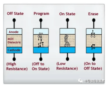
Figure 1: How ReRAM Works
Most commercial industry work, such as the collaboration between TSMC and Infineon, is now centered around OxRAM.
“Both are referred to as resistive RAM because both change the resistance of certain storage elements, but they differ greatly in terms of physics and chemistry,” said Ilan Sever, VP of R&D at Weebit Nano.
“In oxygen vacancies, we apply different voltages in opposite directions across the resistance layer, and then create or dissolve conductive filaments based on the voltage we apply. In this way, we can reset the cell—that is, we dissolve the filaments so it no longer conducts, and the resistance is high. We call it the zero state or reset.”
Kenyon from Intrinsic further explained: “We are changing something in the oxide, and we are creating a filament to bridge the gap between the two electrodes. These devices are very simple capacitive structures, with only one layer of oxide and an electrode on top. We can create a conductive filament bridging the two electrodes. The filament consists of oxygen vacancies. So, we are actually moving some oxygen in the oxide to form the filament and then transitioning from the original high-resistance state to the low-resistance state. When we reverse the polarity, we move the oxygen back in the other direction and re-oxidize a small part of the filament, rather than the entire filament, and then we can move back and forth many, many times between the low-resistance and high-resistance states.”
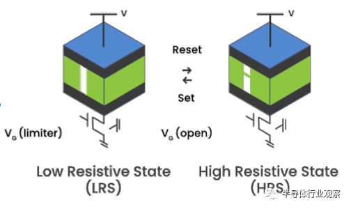
Figure 2: ReRAM Resistance
Potential eFlash Replacement
ReRAM is now one of the main competitors to replace high-end embedded flash (eFlash) series, although it is unlikely to replace NAND flash. As Objective Analysis wrote in its 2023 Emerging Memory Report, “Over time, the NOR embedded in most SoCs will be almost entirely replaced by MRAM, ReRAM, FRAM, or PCM, which will also help drive the success of independent new memories.”
Gary Bronner, Senior Vice President at Rambus Labs, stated, “Compared to embedded flash, ReRAM requires fewer masks to integrate with CMOS processes, can scale down to smaller nodes, and is byte-addressable. The primary metric for traditional NAND flash is cost per bit, whereas ReRAM is not competitive.”
Another example of ReRAM gaining attention is Weebit Nano’s ReRAM, which has now been fully qualified for SkyWater Technology’s 130nm CMOS process.
Additionally, TSMC and Infineon have developed ReRAM (also known as RRAM) together for years, and are now integrating it into automotive microcontrollers.
“A few years ago, as we moved towards advanced process nodes, we believed RRAM was the right choice for embedded memory,” said Sandeep Krishnegowda, VP of Marketing and Applications at Infineon. “It is a low-power technology. It is byte-addressable, so unlike flash, you can write directly. Durability and retention performance are compatible with flash, and the costs are lower. We have been working with TSMC for over a decade to develop RRAM manufacturing technology and algorithms. We first used RRAM in some chip cards used for cashless payments and secure identification. In the consumer industrial market for controllers and MCUs, we use this type of memory as a replacement for embedded flash. Recently, we have brought it into the automotive space.”
For chip cards, ReRAM has another advantage: it is radiation-resistant and has high electromagnetic immunity. “If you consider payment cards and how everyone wants to extract information, you want your memory to be very robust,” Krishnegowda noted.
Moreover, since ReRAM is not charge-based, there are no leakage issues, Kenyon said.
Drawbacks of ReRAM
Like all memory technologies, ReRAM has its vulnerabilities.
Takashi Ando, Chief Research Scientist at IBM, stated, “The fundamental challenge facing ReRAM is that it has more noise than other materials.” “In oxide ReRAM, we randomly move oxygen vacancies. In CBRAM, we randomly use cations. There is some randomness in the operation of the devices, and it comes with high noise, so the inherent noise level is the biggest challenge, but it is more immune to external stimuli compared to MRAM or other memories.”
The impact of noise should not be underestimated. “The biggest issue with ReRAM is its inherent variability (noise) at the single-cell level,” Lin from Synopsys said. “The resistance change from one switching cycle to the next can be as large as the resistance change of a cell group. For filament-based ReRAM, such as OxRAM and CBRAM, the resistance values are controlled by the few oxygen vacancies or metal atoms moving around the filament tip under high electric fields and/or high local temperatures. This process is inherently random, and a few atoms or vacancies can have a significant impact. So, noise is inherent. Increasing the switching current may mitigate variability to some extent, but at the cost of power consumption.”
Kenyon from Intrinsic downplayed this effect. “The traditional industry view is that ReRAM has a variability problem because it is inherent to the process of making these filaments, and there is nothing you can do about it,” he said. “But it really comes down to materials engineering. We have shown that by designing the materials correctly, the variability in programming voltage can be reduced, such as the distribution of different voltages required to transition from high-resistance state to low-resistance state.”
Takeo Tomine, Product Manager at Ansys Totem, also pointed out that heat generation is an issue for ReRAM. “Typically, for advanced technology nodes below 7nm, the device size shrinks while the supply voltage (Vdd) remains constant, leading to higher power density and greater metal density, which generates more heat. Self-heating is a key factor affecting ReRAM reliability and accuracy. When heat gets trapped in the transistor devices, self-heating becomes most severe. For ReRAM, temperature variations reduce the R on/R off ratio, which is detrimental to the accuracy and reliability of many applications, including AI processing. Careful thermal management is needed, especially in designs where power consumption is uneven across different devices. Then, modeling of the heat diffusion generated to nearby layers and devices must be done to capture the full-chip thermal map over time.”
Lin added, “A major challenge for ReRAM technology is the lack of quantitative physical models for multiphysics (i.e., electro-thermal-chemical problems). Empirical models do exist, but there is a lack of fundamental physics. Without good models, it is difficult to control or optimize manufacturing processes.”
In Conclusion
ReRAM’s competitors will not yield without a fight.
“The write times for ReRAM-type technologies are very slow, around 20,000 to 30,000 nanoseconds. SRAM is about 1 or 2 nanoseconds,” said Guedj from Numen. He claimed that Numen’s latest technology can reduce ReRAM write times by 100 times, or Numen’s MRAM can further reduce it to around 50 nanoseconds.
The challenge for MRAM is higher processing costs, which require more technological advancements. This may happen over time to reduce processing costs. Most large foundries will keep their options open, trying both sides and hedging their bets.”
Others believe ReRAM will prevail. Jongsin Yun, memory technology expert at Siemens EDA, stated, “ReRAM has two major advantages over MRAM—simpler processes and a wider read window.” “MRAM requires more than 10 layers of stacking, and all stacks need to be controlled very precisely to form matching crystal proteins. Maintaining high yield is challenging. In contrast, the layer stacking of ReRAM is much simpler and requires relatively less effort to maintain yield. Additionally, the read window (on/off ratio) of MRAM is very narrow, making it prone to failure due to small resistance shifts. On the other hand, ReRAM’s read window is more than an order of magnitude higher, making it less susceptible to parasitic resistance shifts.”
However, in one critical area, MRAM is in the lead, so ReRAM is unlikely to be a suitable choice for last-level cache. Yun stated.
“The typical speed of ReRAM is in the microsecond to hundreds of nanoseconds range, making it unsuitable for use as last-level cache (LLC). As for durability, ReRAM products typically target around 1E5 [100,000 write cycles] of endurance, far below the LLC requirements (1E12 cycles). Due to these limitations, there has been more discussion around MRAM for last-level cache. Adesto, which was later acquired by Dialog Semiconductor and then by Renesas Electronics, demonstrated ReRAM write speeds of up to 10 nanoseconds. In contrast, IBM and Samsung’s joint team demonstrated Mbit MRAM at 250ps, showing significant speed differences,” Yun continued.
For this reason and others, NVM is likely to have multiple options in the foreseeable future.
Ando from IBM stated, “Making NVM suitable for each application rather than a one-size-fits-all dream memory is a more natural thing. My expectation is that we will see NVM customized for each application, and this is already happening in inference and training.”
Finally, Bronner from Rambus noted that both MRAM and ReRAM seem to be gaining attention as embedded memory. “Generally speaking, MRAM appears to have slightly higher performance but also higher costs. ReRAM is cheaper but may not meet the same performance and reliability standards.”
Each technology should be able to find a foothold, depending on the trade-offs that end customers are willing to make.
Original Link

*Disclaimer: This article is original by the author. The content of the article reflects the author’s personal views, and Semiconductor Industry Observation reproduces it only to convey a different perspective. It does not represent Semiconductor Industry Observation’s endorsement or support of this view. If there are any objections, please feel free to contact Semiconductor Industry Observation.
This is the 3535th content shared by Semiconductor Industry Observation. Welcome to follow us.
Recommended Reading
★Interconnection, Becoming Core Technology
★Chip Duopoly, Battle of Chiplets
★Semiconductors, Are There Variables?
Semiconductor Industry Observation

『First Vertical Media in Semiconductors』
Real-time Professional Original Depth
Scan the QR code, reply to the keywords below for more reading
Wafer|Integrated Circuits|Devices|Automotive Chips|Memory|TSMC|AI|Packaging
Reply Submission to see “How to Become a Member of Semiconductor Industry Observation”
Reply Search to easily find other articles you are interested in!