Welcome FPGA engineers to join the official WeChat technical group.
This article mainly introduces the structure, external interfaces, and operations of NOR Flash.
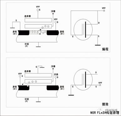
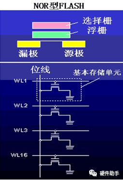
In NOR Flash, the ‘N’ stands for NOT, meaning that when there is a charge in the Floating Gate, it reads ‘0’, and when there is no charge, it reads ‘1’. This is a form of ‘non’ logic; the ‘OR’ means that the various basic storage units under the same Bit Line are connected in parallel, representing ‘or’ logic. This is the origin of NOR.
The characteristic of NOR Flash is that it executes operations in place (eXecute In Place), allowing applications to run directly in Flash without needing to load code into system RAM first.
1. Structure of NOR Flash
In the structure of NOR Flash, every two units share a bit line contact hole and a source line, employing CHE programming and source F-N erasure, which have the advantages of high programming speed and high read speed. However, its programming power consumption is excessive, and in terms of array layout, the contact holes occupy considerable space, resulting in lower integration. It has the following characteristics:
-
Programs and data can be stored on the same chip, with independent data and address buses, allowing for fast random reads. The system can read code directly from Flash without needing to download it to RAM first.
-
It can program one byte or one word, but cannot erase one byte. It must erase by blocks or the entire chip, requiring pre-programming and erasure before reprogramming. It is suitable for storing code, such as for BIOS. Due to the slower erasure and programming speeds of NOR Flash, and the large block size, the time taken for these operations can be lengthy. In applications for pure data storage and file storage, NOR technology is inadequate.
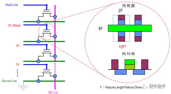

From the perspective of supported minimum access units, NOR Flash is generally divided into 8-bit and 16-bit types. For an 8-bit NOR Flash chip, or a chip operating in 8-BIT mode, one address corresponds to one BYTE (8-BIT) of data. For example, an 8-BIT NOR Flash with a capacity of 4 BYTES should have 8 data signals D7-D0 and 2 address signals A1-A0. Address 0x0 corresponds to the 0th BYTE, address 0x1 corresponds to the 1st BYTE, address 0x2 corresponds to the 2nd BYTE, and address 0x3 corresponds to the 3rd BYTE.
For a 16-bit NOR Flash chip, or a chip operating in 16-BIT mode, one address corresponds to one HALF-WORD (16-BIT) of data. For example, a 16-BIT NOR Flash with a capacity of 4 BYTES should have 16 data signal lines D15-D0 and 1 address signal A0. Address 0x0 corresponds to the 0th HALF-WORD inside the chip, while address 0x1 corresponds to the 1st HALF-WORD. The 8-BIT mode has one more address line than the 16-BIT mode but has 8 fewer data lines, generally reusing the address line DQ15.
NOR Flash is generally divided into multiple SECTORS, with each SECTOR including a certain number of storage units. For some large-capacity Flash, it is also divided into different BANKS, with each BANK containing a certain number of SECTORS. The erasure operation of NOR Flash is generally performed in units of SECTOR, BANK, or the entire Flash chip.
2. Parallel NOR Flash
2.1. NOR Flash Pins
|
Pin |
Definition |
|
VDD |
Operating Voltage |
|
VSS |
Ground |
|
DQn |
Data Line |
|
An |
Address Line |
|
DQ15/A-1 |
DQ15/A-1 LSB Address (the address line differs by one between 8-bit mode and 16-bit mode, achieved through multiplexing) |
|
WE# |
Write Enable |
|
OE# |
Output Enable |
|
CS# |
Chip Select |
|
RESET# |
Reset Signal |
|
BYTE# |
Data Width Select |
|
RY/BY# |
Ready/Busy |
|
ACC/WP# |
Acceleration/Write Protect |
2.2. NOR Flash Operation States
|
CEn |
OEn |
WEn |
RESETn |
ACC/WP# |
ADDRESS |
DQ[7:0] |
BYTEn |
||
|
L |
H |
||||||||
|
DQ[15:8] |
|||||||||
|
Read |
L |
L |
H |
H |
x |
IN |
OUT |
DQ[14:8]=High-Z DQ15=A-1 (multiplexed) |
OUT |
|
Write |
L |
H |
L |
H |
IN |
IO |
IO |
||
|
Acc Program |
L |
H |
L |
H |
Vhh(12±0.5V) high programming voltage |
IN |
IO |
IO |
|
|
Output Disable |
L |
H |
H |
H |
x |
x |
High-Z |
High-Z |
High-Z |
|
Standby |
VCC±0.3V |
x |
x |
VCC±0.3V |
H |
x |
High-Z |
High-Z |
High-Z |
|
Reset |
x |
x |
x |
L |
x |
x |
High-Z |
High-Z |
High-Z |
After powering on, NOR Flash is in the data reading state (Reading Array Data). This state allows for normal read operations, similar to reading from SDRAM/SRAM/ROM. (If it were different, how would the chip read the boot code from NOR Flash after powering on?)
NOR Flash has a memory-like interface, allowing it to read like memory but not write like memory; writing and erasing NOR Flash requires specific commands. When discussing NOR Flash, it usually involves the CFI (Common Flash Interface). Generally, NOR Flash supports commands to read manufacturer ID and device ID, but not all NOR Flash supports commands to obtain information such as the chip’s capacity, number of sectors, and block size for erasure. To improve compatibility for future NOR Flash, the CFI interface was introduced, embedding relevant information into the chip, which can be accessed via CFI commands.
Before performing operations on Flash, it is common to read the chip information, such as the device ID number. The main purpose of this is to determine whether the program written is compatible with the device. NOR Flash supports two methods for obtaining the ID number. One method is used by programmers requiring high voltage (11.5V-12.5V). The other method is the so-called in-system method, which completes the process through the NOR Flash command register within the system. The in-system method requires switching to the automatic selection (Autoselect Command) mode, which must be accomplished by sending a command. After entering the automatic selection (Autoselect Command) mode, a reset command must be sent to return to the data reading state (Reading Array Data).
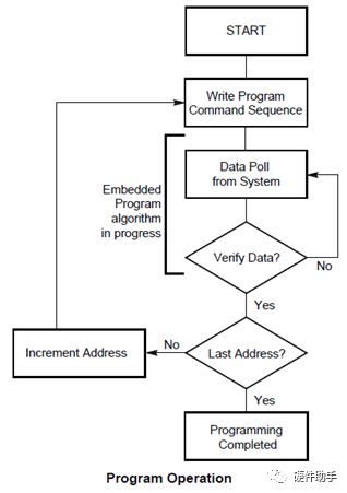
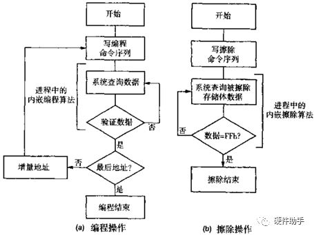
After obtaining the information, data erasure is typically required. NOR Flash supports sector erase (Sector Erase) and chip erase (Chip Erase). Both modes have corresponding command sequences. After completing the erase command, it will automatically return to the data reading (Reading Array Data) state. Before returning, the programming status can be queried.
After erasure is completed, the chip must undergo a write operation, known as programming. This requires entering the programming (Program) state. After completing the programming command, it will automatically return to the data reading (Reading Array Data) state. Before returning, the programming status can be queried. Note: Always erase before programming, as programming can only rewrite ‘1’ to ‘0’; through erasure, all data can be rewritten to ‘1’.
2.2.1. Sector Erase
NOR Flash supports sector erase (Sector Erase) and chip erase (Chip Erase). Both modes have corresponding command sequences. After completing the erase command, it will automatically return to the data reading (Reading Array Data) state. Before returning, the programming status can be queried.
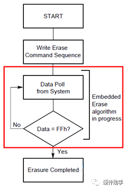
The Embedded Erase algorithm refers to the “embedded erase algorithm program”; when the erase command is issued, NOR Flash will execute a series of instructions internally to perform the erase operation. During this process, it checks Data=FF? to determine the erase status, but this is an internal judgment method of NOR Flash. Correspondingly, the external memory controller can detect it through Data#Polling.
2.2.2. Programming (Program)
After erasure, the chip must undergo a writing operation, known as programming. This requires entering the programming (Program) state. After completing the programming command, it will automatically return to the data reading (Reading Array Data) state. Before returning, the programming status can be queried. Note: Always erase before programming, as programming can only rewrite ‘1’ to ‘0’; through erasure, all data can be rewritten to ‘1’.
2.2.3. Write Operation Status (WRITE OPERATION STATUS)
NOR Flash provides several data bits to determine the status of a write operation, which are: DQ2, DQ3, DQ5, DQ6, DQ7, and RY/BY#. Each of DQ7, RY/BY#, and DQ6 provides a method to determine whether a programming or erasing operation has been completed or is ongoing. In actual programming, only one of these needs to be used.
-
DQ7: Data# Polling bit, in the programming process, the data read from the address being programmed has DQ7 as the complement of the data to be written. For example, if the data being written is 0x0000, then the input DQ7 is 0, and the data read during programming is 1; when programming is completed, the data read returns to the input data 0. During erasure, DQ7 outputs 0; after erasure is completed, it outputs 1; note that the address read must be within the erased range. RY/BY#: High level indicates ‘ready’, low level indicates ‘busy’.
-
DQ6: Toggle Bit 1, during programming and erasure, reading any address will cause DQ6 to toggle (between 0 and 1). When the operation is completed, DQ6 stops toggling.
-
DQ2: Toggle Bit 2, when a sector is selected for erasure, reading a valid address (within the erased sector range) will cause DQ2 to toggle. DQ2 can only determine whether a specific sector is selected for erasure but cannot distinguish whether this sector is currently being erased or is in a paused state. In contrast, DQ6 can distinguish whether NOR Flash is being erased or is in a paused state but cannot determine which sector is selected for erasure. Therefore, these two bits are needed to determine sector and mode status information.
-
DQ5: Timeout Bit (Exceeded Timing Limits), when a programming or erasure operation exceeds a specific internal pulse count, DQ5=1 indicates that the operation has failed. When programming, changing 0 to 1 causes DQ5=1, as only an erase operation can change 0 to 1. When an error occurs, a reset command must be executed to return to the read data state.
-
DQ3: Sector Erase Timer, only active during sector erase commands. When the erase command truly begins working, DQ3=1, at which point all input commands (except the erase pause command) are ignored; when DQ3=0, additional sectors can be added for multi-sector erasure.
3. Serial NOR Flash
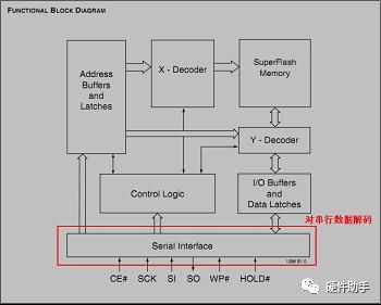
The main interface of Serial NOR Flash is the SPI interface, and its internal storage matrix access and storage structure are consistent with parallel NOR Flash, just with an additional serial interface for decoding serial data.
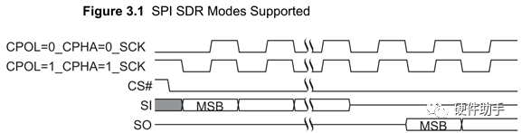
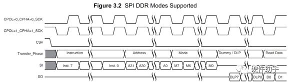
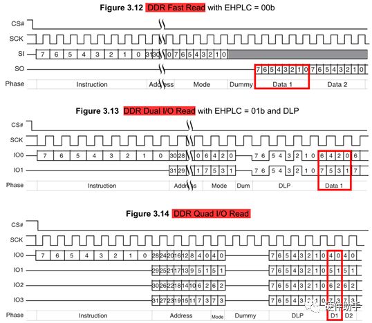
3.1. SPI SDR/DDR Sampling Methods
SPI’s SCK supports single edge triggering and double edge triggering; in single edge triggering, it triggers only on the rising or falling edge, while in double edge triggering, it triggers on both the rising and falling edges.
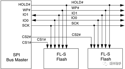
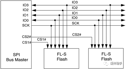
3.2. SPI x1/2/4 Connection Methods
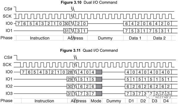
SPI supports 1-bit, 2-bit, and 4-bit data transfer widths.
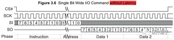
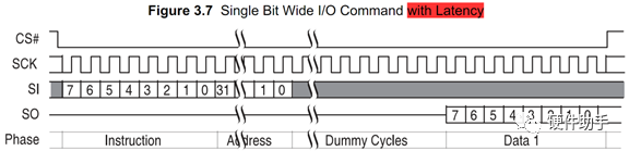
Traditional SPI single bit wide commands (Single or SIO) send information from the host to the memory only on the SI signal. Data may be sent back to the host serially on the Serial Output (SO) signal.
Dual or Quad Output commands send information from the host to the memory only on the SI signal. Data will be returned to the host as a sequence of bit pairs on IO0 and IO1 or four bit (nibble) groups on IO0, IO1, IO2, and IO3.
Dual or Quad Input/Output (I/O) commands send information from the host to the memory as bit pairs on IO0 and IO1 or four bit (nibble) groups on IO0, IO1, IO2, and IO3. Data is returned to the host similarly as bit pairs on IO0 and IO1 or four bit (nibble) groups on IO0, IO1, IO2, and IO3.


Welcome communication engineers and FPGA engineers to follow our public account.

FPGA WeChat Technical Group
Welcome everyone to join the national FPGA WeChat technical group, where there is a group of engineers passionate about technology, and we can discuss technology together!

Press and hold to join the national FPGA technical group.
FPGA Technical Group Platform Self-operated: Xilinx Altera Micron, Samsung, Hynix, ADI, TI, ST, NXP, and other brand advantage agents and distributors. If you need any models, please send us your list, and we will provide you with the most competitive quotation in the first instance! Prices are more than 5% lower than your original supplier! Welcome to inquire – WeChat: 1051197468 or directly send your needs to the group owner.
Official thanks to brands in the FPGA technical group: Xilinx, Intel (Altera), Microsemi (Actel), Lattice, Vantis, Quicklogic, Lucent, etc.