Skip to content
This article highlights: 1. Common FLASH reference circuits from Huawei, Samsung, and Intel; 2. Explanation of 2-bit and 4-bit NAND FLASH in conjunction with datasheets; 3. Summary of debugging thoughts and sharing of simple debugging experiences; 4. Introduction to the latest 3D Xpoint technology.
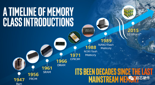
First, I would like to use this image to illustrate the development process of memory over the past 70 years. Throughout these 70 years, we can observe significant leaps in capacity, speed, and lifespan.
Next, I will present several common application circuits in practical engineering.
(1) First Application: The engineering application circuits of NOR FLASH and NAND FLASH are shown in the figure below. The circuit structure is quite simple and is a very commonly used circuit unit, so I won’t elaborate further.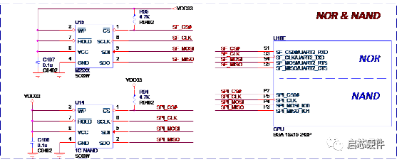 (2) Second Application There is another commonly used application circuit, which is often used in current practical engineering, that is, the application unit circuit of 2-bit or 4-bit NAND FLASH. When hardware engineers select components, one of the specifications is to choose between X1/X2/X4, which is used to select the number of bits. The circuit form is slightly different, as shown in the figure below.
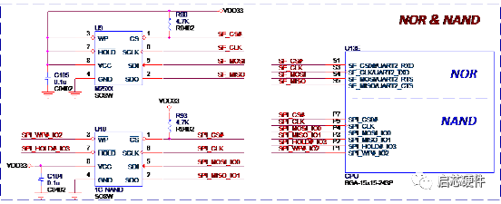 As shown in the figure, several pins are reused, and combined with MISO and MISO, they form D0, D1, D2, and D3. Specific details can be found in the device SPEC, as shown in the figure below.
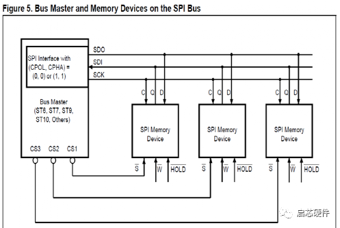
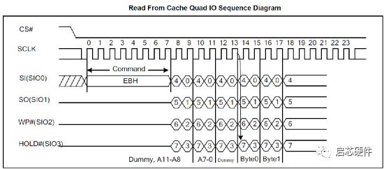 (3) Third Application This application is also very common, as shown in the figure below, which is a schematic diagram of multiple SPI FLASH chips connected to the CPU through different chip select signals. It is quite simple, but it is a commonly used circuit module that must be remembered.
[Debugging Experience] I would like to share an experience from early debugging of an SPI FLASH on a motherboard.
1. After soldering a new SPI FLASH on the motherboard, the external ROM chip never worked, and the soldering seemed fine.
(3) Third Application This application is also very common, as shown in the figure below, which is a schematic diagram of multiple SPI FLASH chips connected to the CPU through different chip select signals. It is quite simple, but it is a commonly used circuit module that must be remembered.
[Debugging Experience] I would like to share an experience from early debugging of an SPI FLASH on a motherboard.
1. After soldering a new SPI FLASH on the motherboard, the external ROM chip never worked, and the soldering seemed fine.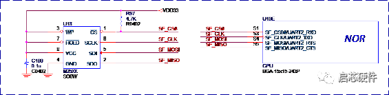 After repeated checks, it was found that the main system primarily used a 1.8V power supply, while the SPI ROM required a 3.3V power supply. If using the 25XX chip, a Level Shift circuit is required. Alternatively, the second option is to use Winbond’s 1.8V chip W25Q32XX, which made the system work after replacing this chip.
[New Technology Progress] 3D Xpoint is the most groundbreaking storage technology since NAND Flash was introduced. It is over 1000 times faster than NAND and has a lifespan over 1000 times that of NAND. Additionally, it has the following four advantages, making 3D Xpoint seen as a disruptor in the storage industry: (1) 1000 times faster than NAND Flash; (2) Cost is only half that of DRAM; (3) Lifespan is 1000 times that of NAND; (4) Density is 10 times that of traditional storage;
After repeated checks, it was found that the main system primarily used a 1.8V power supply, while the SPI ROM required a 3.3V power supply. If using the 25XX chip, a Level Shift circuit is required. Alternatively, the second option is to use Winbond’s 1.8V chip W25Q32XX, which made the system work after replacing this chip.
[New Technology Progress] 3D Xpoint is the most groundbreaking storage technology since NAND Flash was introduced. It is over 1000 times faster than NAND and has a lifespan over 1000 times that of NAND. Additionally, it has the following four advantages, making 3D Xpoint seen as a disruptor in the storage industry: (1) 1000 times faster than NAND Flash; (2) Cost is only half that of DRAM; (3) Lifespan is 1000 times that of NAND; (4) Density is 10 times that of traditional storage; Because of these advantages, it centrally addresses the pain points currently existing in memory.
1. Memory performance is currently a shortcoming in PC devices.
2. DRAM: Volatile and difficult to solve, meaning it requires continuous power supply; data will be lost if power is cut. DRAM only continuously adjusts values on the bus, and the core storage architecture changes little.
3. NAND: Lifespan and latency are unsatisfactory; even the best performing SLC NAND particles have a lifespan much shorter than DRAM.
Because of these advantages, it centrally addresses the pain points currently existing in memory.
1. Memory performance is currently a shortcoming in PC devices.
2. DRAM: Volatile and difficult to solve, meaning it requires continuous power supply; data will be lost if power is cut. DRAM only continuously adjusts values on the bus, and the core storage architecture changes little.
3. NAND: Lifespan and latency are unsatisfactory; even the best performing SLC NAND particles have a lifespan much shorter than DRAM. The fastest DDR4 memory still can only serve as a temporary storage.
Brief Explanation of Principles: The working principle of 3D XPoint fundamentally differs from that of NAND. NAND captures different quantities of electrons through an insulated floating gate to define bit values, whereas 3D XPoint is a resistive-based storage technology that distinguishes between 0 and 1 by changing the resistance level of the unit.
The fastest DDR4 memory still can only serve as a temporary storage.
Brief Explanation of Principles: The working principle of 3D XPoint fundamentally differs from that of NAND. NAND captures different quantities of electrons through an insulated floating gate to define bit values, whereas 3D XPoint is a resistive-based storage technology that distinguishes between 0 and 1 by changing the resistance level of the unit.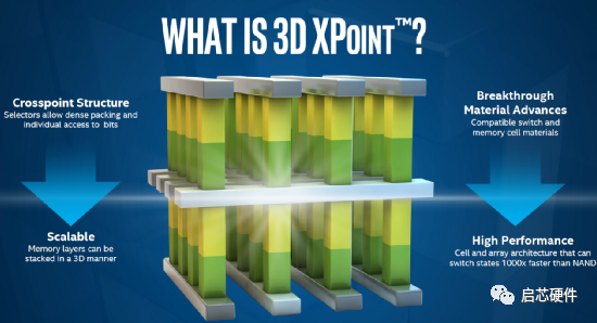 The storage units of 3D XPoint can be stacked in 3D, further enhancing storage density. According to Intel’s official promotion, 3D XPoint has NAND-like capacity and DRAM-like performance, including being over 1000 times faster than NAND (which should refer to lower latency), with a lifespan over 1000 times that of NAND, and data density reaching over ten times that of DRAM. Such amazing performance, are you afraid?
Below are the application debugging notes for NAND and NOR Flash:
For NAND Flash, its operations include erasing and programming, with the minimum unit for erasing being a block and for programming being a page. Since the size of a page is much smaller than that of a block, the read, write, and erase speeds of NAND Flash are much faster than those of NOR Flash, while the erase operation is slower than the read operation.
For NOR Flash, its operations also include erasing and programming, with the minimum units for both being bits. The read speed of NOR Flash is much faster than that of NAND Flash, but the bit-level erasing and programming operations are very slow, making the erase and programming speeds of NOR Flash much slower than those of NAND Flash.
When using NAND or NOR Flash, attention must be paid to the details of their erase and programming operations, such as the minimum units for erasing and programming, and the speeds of these operations. Additionally, other parameters such as address mapping, capacity, and interface type must also be considered.
When using NAND or NOR Flash, bad block management and data protection are necessary. For bad block management, this can be achieved by testing and recording bad block locations before leaving the factory; for data protection, methods such as backup and verification can be employed to ensure data safety.
When using NAND or NOR Flash, attention should be paid to the design of hardware circuits such as power supply and clock to ensure normal operation. Furthermore, software debugging and optimization are required to ensure the correctness and performance of the program.
In summary, when using NAND or NOR Flash, it is essential to pay attention to operational details and other parameters, as well as to perform bad block management and data protection to ensure normal operation and data safety.
The storage units of 3D XPoint can be stacked in 3D, further enhancing storage density. According to Intel’s official promotion, 3D XPoint has NAND-like capacity and DRAM-like performance, including being over 1000 times faster than NAND (which should refer to lower latency), with a lifespan over 1000 times that of NAND, and data density reaching over ten times that of DRAM. Such amazing performance, are you afraid?
Below are the application debugging notes for NAND and NOR Flash:
For NAND Flash, its operations include erasing and programming, with the minimum unit for erasing being a block and for programming being a page. Since the size of a page is much smaller than that of a block, the read, write, and erase speeds of NAND Flash are much faster than those of NOR Flash, while the erase operation is slower than the read operation.
For NOR Flash, its operations also include erasing and programming, with the minimum units for both being bits. The read speed of NOR Flash is much faster than that of NAND Flash, but the bit-level erasing and programming operations are very slow, making the erase and programming speeds of NOR Flash much slower than those of NAND Flash.
When using NAND or NOR Flash, attention must be paid to the details of their erase and programming operations, such as the minimum units for erasing and programming, and the speeds of these operations. Additionally, other parameters such as address mapping, capacity, and interface type must also be considered.
When using NAND or NOR Flash, bad block management and data protection are necessary. For bad block management, this can be achieved by testing and recording bad block locations before leaving the factory; for data protection, methods such as backup and verification can be employed to ensure data safety.
When using NAND or NOR Flash, attention should be paid to the design of hardware circuits such as power supply and clock to ensure normal operation. Furthermore, software debugging and optimization are required to ensure the correctness and performance of the program.
In summary, when using NAND or NOR Flash, it is essential to pay attention to operational details and other parameters, as well as to perform bad block management and data protection to ensure normal operation and data safety.