Source: Content compiled from Semiconductor Industry Observer (ID: icbank) from eejournal, thank you.
Before the semiconductor version emerged, ancient people tried various forms of computer memory. I think we can say that water-based capacitors provided a form of memory for the national income monetary simulation computer (MONIAC) manufactured in the UK in 1949. Notably, MONIAC inspired Glooper (also known as “the thing in the cellar”) in Terry Pratchett’s Discworld. Similarly, as discussed in a 1964 article, electronic capacitors can serve as storage elements in electronic analog computers. Now I wonder if mechanical analog computers had something similar.
In terms of digital computers, Konrad Zuse’s mechanical Z1 computer had a purely mechanical digital memory (this meticulously handcrafted binary floating-point machine was put into use in Berlin around 1938, just in time to be destroyed during WWII). Later digital machines used various technologies to implement storage systems, including rotating capacitors and magnetic drums, vacuum tubes and Williams tubes, relays, and mercury delay lines, etc.
Perhaps because I like blowing bubbles (who doesn’t?), I have always been fond of those small but vibrant magnetic bubble memory modules, which left us too soon. Additionally, I have a fondness for large-capacity storage forms such as punched paper products (cards and tapes), magnetic tapes, and magnetic hard disk drives (HDD).
Of course, we eventually developed semiconductor storage devices such as SRAM, DRAM, EPROM, EEPROM, and flash memory. There are also some other competitors, including phase-change memory (PCM, also known as PRAM), magnetic RAM (MRAM), ferroelectric RAM (FRAM or FeRAM), and resistive RAM (ReRAM), and these are just the beginning, but let’s not go too far.
Among all the aforementioned technologies, three main technologies are SRAM, DRAM, and flash memory. All DDR (Double Data Rate) and HBM (High Bandwidth Memory) are based on DRAM. Flash memory mainly comes in two types: NAND flash and NOR flash.
Due to the mistaken belief that NOR flash was about to be phased out, many manufacturers decided to exit this field a decade ago. Unfortunately, they left too early, as more and more applications and markets began to leverage the advantages offered by NOR flash. As a result, by 2020, Macronix, which held onto the belief in NOR flash, found itself with a 24% share of the NOR flash market. Even better, this market has a compound annual growth rate of 15%, expected to continue until 2025 and beyond. During this challenging time, it is even more reassuring that Macronix has completed all wafer manufacturing in-house using its 200mm and 300mm fabs (lucky guys).
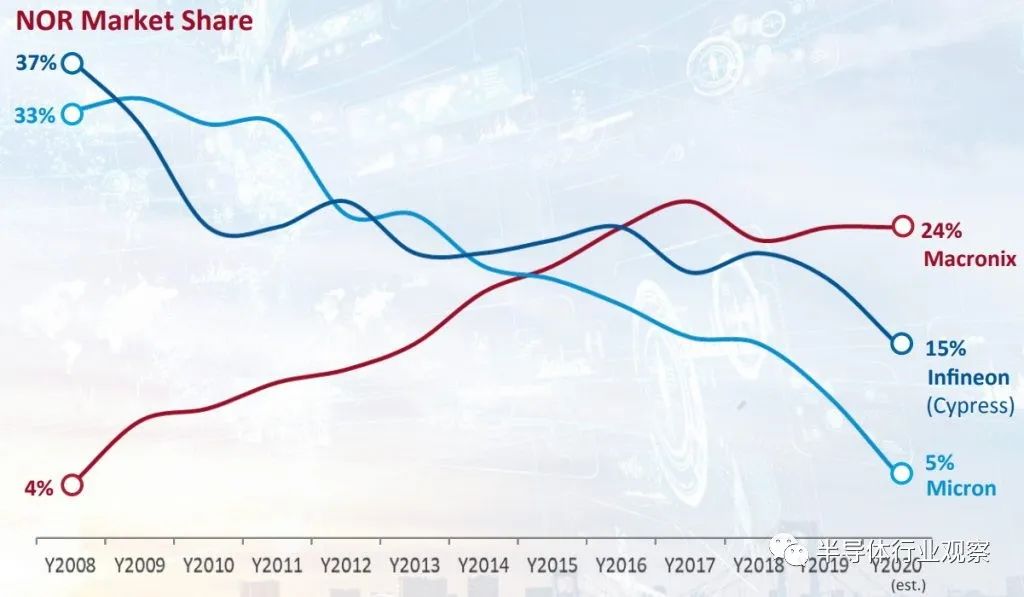
By 2020, Macronix had taken the lead in the NOR market
(Image Source: Macronix, Data Source: Omdia (iHS Market) Omdia (iHS Market) and Macronix Marketing)
So, is NOR flash better than NAND flash? The answer is “yes,” “no,” or “maybe,” depending on what you want to do with it. I should also point out that Macronix offers both NOR and NAND products, so they have no bias towards either (except for the fact that they are the leaders in the NOR flash market, LOL).
In short, compared to NOR flash, NAND flash has much smaller cell sizes, much faster write and erase speeds, and much higher capacity/density. In contrast, NOR flash has true random access capability and faster read speeds, making it an ideal choice for executing code. Additionally, NOR flash is more reliable than NAND flash and has better data retention capabilities.
NAND and NOR flash each have their advantages and disadvantages, and preferences vary in application areas. In particular, NAND flash is favored for large-capacity data storage deployments, while NOR flash shines in code storage and execution tasks.
The key point here is that users appreciate the fast access time of NOR flash (about 100ns for NOR flash compared to about 100us for TLC NAND flash), its simplicity (a simple SPI interface compared to the complex controller dependency of NAND flash), and the fact that automotive-grade NOR flash is available.
This all reminds me of my recent chat with Anthony Le, Vice President of Marketing at Macronix USA. Anthony told me that his colleagues are leveraging their mature experience in 3D NAND to develop a next-generation 3D NOR flash device to extend their 2D NOR flash products.
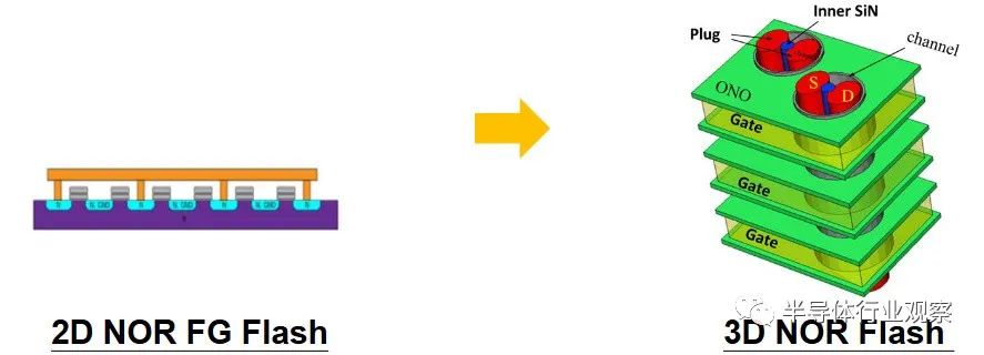
Transitioning from 2D NOR to 3D NOR (Source: Macronix)
It is important to note that the 3D we are referring to is about 3D process stacking technology, not 3D chip stacking technology. Macronix is currently developing a 32-layer 3D NOR flash production line, whose memory density will be 7 times that of 2D NOR flash. In the future, Macronix may use hundreds of layers to further increase density. Similar to existing 2D NOR flash, these 3D NOR flash devices will be divided into industrial grade and automotive grade (AEC).
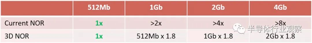
Initial Pricing Strategy (Source: Macronix)
What does all this mean? Please look at the initial pricing strategy table above. The current NOR “row” refers to existing 2D NOR flash.
The goal here is to compare the cost-effectiveness of 2D and 3D NOR flash. The current 2D NOR flash at 1x has been standardized. It doesn’t matter which supplier you are talking about (Macronix, Micron, Infineon). For example, I just found a 512Mb NOR flash on Mouser for about $1.
If you want to obtain a 1Gb NOR flash using existing 2D technology, you must stack two 512Mb 2D dice, which means the cost doubles. The reason the table shows “>2 times” is that stacking dice also incurs costs, but we are focusing on the cost of the wafers here. Similarly, a 2Gb NOR flash requires stacking 4 of the 512Mb 2D dice (4 times the cost of 512Mb), while a 4Gb NOR flash requires stacking 8 of the 512Mb 2D dice (8 times the cost of 512Mb).
In contrast, with 3D NOR, all functions are implemented on a single chip. This is why Micronix adopts the initial pricing strategy shown in the figure. The price of a 1Gb chip is 1.8 times that of a 512Mb chip, the price of a 2Gb chip is 1.8 times that of a 1Gb chip, and the price of a 4Gb chip is 1.8 times that of a 2Gb chip. Moreover, there are no additional chip stacking costs because… well… we don’t stack chips. Assuming the price of a 512Mb 3D die is $1, then the price of a 4Gb die would be $1 x 1.8 x 1.8 x 1.8 = $5.8 (whereas the stacking price of 8 of the 512Mb 2D dies would be $8). Reflecting on how automotive manufacturers are keen on counting money, I can only imagine how bright their eyes would be upon hearing this news.
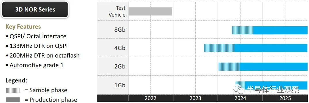
3D NOR Flash Product Plan (Source: Macronix)
I know what you are thinking: “Stop daydreaming! When can I get my hands on these little beauties?” The above image reveals everything. Notably, as I write this, the 4Gb parts are also in sampling, just as you read these words.
Click the link at the end of the article 【Read Original】 to view the original link.

*Disclaimer: This article is original by the author. The content of the article is the author’s personal opinion, and Semiconductor Industry Observer reproduces it only to convey a different viewpoint, which does not represent Semiconductor Industry Observer’s endorsement or support of that viewpoint. If there are any objections, please feel free to contact Semiconductor Industry Observer.
This is the 3567th issue shared by “Semiconductor Industry Observer” for you, welcome to follow.
Recommended Reading
★DRAM, Where To? Where From?
★iPhone 15, What Chips Are Used?
★Semiconductor Industry, Roadmap for the Next Decade
Semiconductor Industry Observer

“The First Vertical Media in the Semiconductor Industry“
Real-time Professional Original Depth
Scan the QR code, reply to the keywords below to read more
Wafer|Integrated Circuit|Equipment|Automotive Chips|Storage|TSMC|AI|Packaging
Reply Submission to see “How to Become a Member of the Semiconductor Industry Observer”
Reply Search to easily find other articles you are interested in!