
At the beginning of project development, we select chips that meet the design requirements. Among these, RAM determines the memory size during program execution, while ROM determines the storage space for applications. However, for projects with particularly large application functions, the internal FLASH (ROM) storage space of the MCU may not be sufficient. At this point, external program storage space is needed, and NOR FLASH is one such solution.
This article provides a detailed introduction and explanation of the technical points involved, covering the following four main contents:
1. KEIL Download Program Configuration and Explanation
By configuring the project, KEIL generates the corresponding HEX or BIN format programming files after compiling the project. After clicking the Download button, the programming file will be burned into the chip.
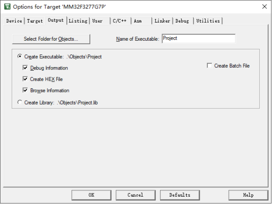
Click the Option for Target magic wand button, and in the Output tab of the popped-up Option for Target window, set the generated programming file name and check the Create HEX file option, as shown in the figure below:
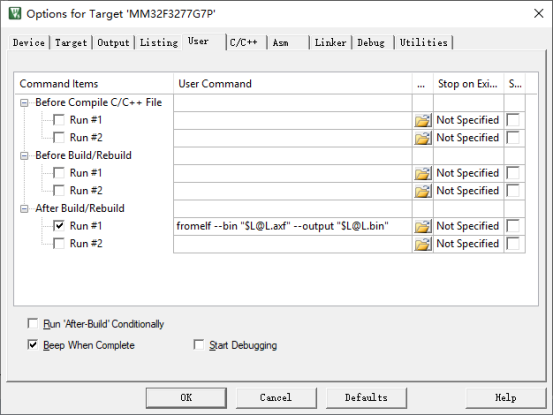
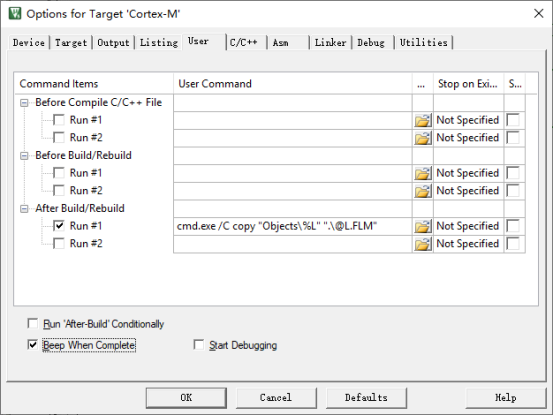
If you also need to generate a BIN format programming file, you can configure it in the User tab as shown in the figure below:
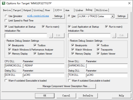
Next, select the appropriate debugging download tool in the Debug tab.
In the Utilities tab, configure the download settings (using the same tool as Debug to download the program), as shown in the figure below:
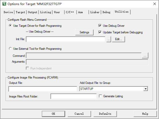
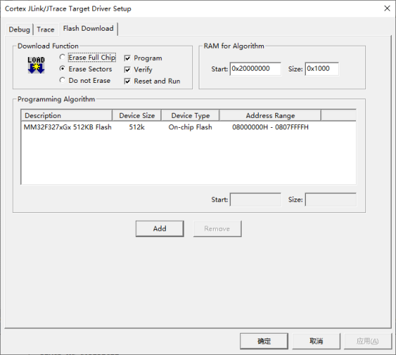
Additionally, in the Utilities tab, click the Settings button and in the popped-up window, configure the Flash Download tab as shown below:
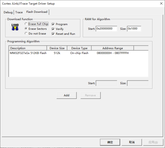
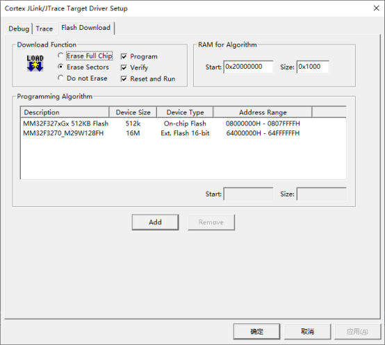
Download Function Settings: This includes the selection for erase, programming, verification, and resetting the chip after download completion to run the application.
Programming (Download) Algorithm Selection: Generally, after selecting the corresponding chip when creating the project, the download algorithm is set by default. If it is not available, we can click the ADD button to add the corresponding download algorithm; the download algorithm lists the description, device storage size, device type, and address range.
Programming (Download) Algorithm Position in RAM: This is generally default; START indicates the starting address of the chip RAM, which is determined by the chip; SIZE indicates the maximum supported programming (download) algorithm program space size, which can be modified but must not be less than the download algorithm program size.
Once all configurations are complete, we compile the project code without error warnings, and click the Download button to download the application program to the chip.
So, after clicking the Download button, how does KEIL download the programming file to the chip?
In simple terms, KEIL software loads the programming (download) algorithm into the specified RAM space of the chip (this space is the aforementioned RAM space with START as the starting address and SIZE as the size), and runs the download algorithm to parse the download file, writing the necessary data to the specified storage address via the download algorithm, completing the programming process.
2. MM32 Implementation of Jumping to NOR FLASH to Run Programs
The MM32F3270 series MCUs support the FSMC feature for memory control, allowing configurable static memory including SRAM and NOR FLASH; it also supports 8080/6800 interfaces, which can be applied to LCD displays.
The reason NOR FLASH can run programs is primarily because its internal address/data lines are separate, supporting byte access and meeting the requirements for CPU instruction decoding and execution (the instruction code is stored on NOR FLASH; the MCU provides an address to NOR FLASH, which returns the corresponding data at that address to the MCU for execution, without any additional processing operations in between).
Thus, to implement jumping to NOR FLASH to run programs using MM32, we only need to perform the FSMC initialization configuration between NOR FLASH and the MCU and the program jump based on running from MM32’s internal FLASH. The specific reference code is as follows:
FSMC Initialization Configuration:
/*******************************************************************************
 * @file    NOR.c
 * @author  King
 * @version V1.00
 * @date    25-Jan-2021
 * @brief   ......
*******************************************************************************/


/* Define to prevent recursive inclusion -------------------------------------*/
#define __NOR_C__


/* Includes ------------------------------------------------------------------*/
#include "NOR.h"


/* Private typedef -----------------------------------------------------------*/
/* Private define ------------------------------------------------------------*/
/* Private macro -------------------------------------------------------------*/
/* Private variables ---------------------------------------------------------*/
/* Private function prototypes -----------------------------------------------*/
/* Private functions ---------------------------------------------------------*/


/* Exported variables --------------------------------------------------------*/
/* Exported function prototypes ----------------------------------------------*/


/*******************************************************************************
 * @brief
 * @param
 * @retval
 * @attention
*******************************************************************************/
void NOR_InitGPIO(void)
{
    GPIO_InitTypeDef GPIO_InitStructure;


    RCC_AHBPeriphClockCmd(RCC_AHBPeriph_GPIOD | RCC_AHBPeriph_GPIOE |
                          RCC_AHBPeriph_GPIOF | RCC_AHBPeriph_GPIOG , ENABLE);


    GPIO_PinAFConfig(GPIOD, GPIO_PinSource14, GPIO_AF_12);  /* FSMC_D0  */
    GPIO_PinAFConfig(GPIOD, GPIO_PinSource15, GPIO_AF_12);  /* FSMC_D1  */
    GPIO_PinAFConfig(GPIOD, GPIO_PinSource0,  GPIO_AF_12);  /* FSMC_D2  */
    GPIO_PinAFConfig(GPIOD, GPIO_PinSource1,  GPIO_AF_12);  /* FSMC_D3  */
    GPIO_PinAFConfig(GPIOE, GPIO_PinSource7,  GPIO_AF_12);  /* FSMC_D4  */
    GPIO_PinAFConfig(GPIOE, GPIO_PinSource8,  GPIO_AF_12);  /* FSMC_D5  */
    GPIO_PinAFConfig(GPIOE, GPIO_PinSource9,  GPIO_AF_12);  /* FSMC_D6  */
    GPIO_PinAFConfig(GPIOE, GPIO_PinSource10, GPIO_AF_12);  /* FSMC_D7  */
    GPIO_PinAFConfig(GPIOE, GPIO_PinSource11, GPIO_AF_12);  /* FSMC_D8  */
    GPIO_PinAFConfig(GPIOE, GPIO_PinSource12, GPIO_AF_12);  /* FSMC_D9  */
    GPIO_PinAFConfig(GPIOE, GPIO_PinSource13, GPIO_AF_12);  /* FSMC_D10 */
    GPIO_PinAFConfig(GPIOE, GPIO_PinSource14, GPIO_AF_12);  /* FSMC_D11 */
    GPIO_PinAFConfig(GPIOE, GPIO_PinSource15, GPIO_AF_12);  /* FSMC_D12 */
    GPIO_PinAFConfig(GPIOD, GPIO_PinSource8,  GPIO_AF_12);  /* FSMC_D13 */
    GPIO_PinAFConfig(GPIOD, GPIO_PinSource9,  GPIO_AF_12);  /* FSMC_D14 */
    GPIO_PinAFConfig(GPIOD, GPIO_PinSource10, GPIO_AF_12);  /* FSMC_D15 */


    GPIO_PinAFConfig(GPIOF, GPIO_PinSource0,  GPIO_AF_12);  /* FSMC_A0  */
    GPIO_PinAFConfig(GPIOF, GPIO_PinSource1,  GPIO_AF_12);  /* FSMC_A1  */
    GPIO_PinAFConfig(GPIOF, GPIO_PinSource2,  GPIO_AF_12);  /* FSMC_A2  */
    GPIO_PinAFConfig(GPIOF, GPIO_PinSource3,  GPIO_AF_12);  /* FSMC_A3  */
    GPIO_PinAFConfig(GPIOF, GPIO_PinSource4,  GPIO_AF_12);  /* FSMC_A4  */
    GPIO_PinAFConfig(GPIOF, GPIO_PinSource5,  GPIO_AF_12);  /* FSMC_A5  */


    GPIO_PinAFConfig(GPIOF, GPIO_PinSource12, GPIO_AF_12);  /* FSMC_A6  */
    GPIO_PinAFConfig(GPIOF, GPIO_PinSource13, GPIO_AF_12);  /* FSMC_A7  */
    GPIO_PinAFConfig(GPIOF, GPIO_PinSource14, GPIO_AF_12);  /* FSMC_A8  */
    GPIO_PinAFConfig(GPIOF, GPIO_PinSource15, GPIO_AF_12);  /* FSMC_A9  */


    GPIO_PinAFConfig(GPIOG, GPIO_PinSource0,  GPIO_AF_12);  /* FSMC_A10 */
    GPIO_PinAFConfig(GPIOG, GPIO_PinSource1,  GPIO_AF_12);  /* FSMC_A11 */
    GPIO_PinAFConfig(GPIOG, GPIO_PinSource2,  GPIO_AF_12);  /* FSMC_A12 */
    GPIO_PinAFConfig(GPIOG, GPIO_PinSource3,  GPIO_AF_12);  /* FSMC_A13 */
    GPIO_PinAFConfig(GPIOG, GPIO_PinSource4,  GPIO_AF_12);  /* FSMC_A14 */
    GPIO_PinAFConfig(GPIOG, GPIO_PinSource5,  GPIO_AF_12);  /* FSMC_A15 */


    GPIO_PinAFConfig(GPIOD, GPIO_PinSource11, GPIO_AF_12);  /* FSMC_A16 */
    GPIO_PinAFConfig(GPIOD, GPIO_PinSource12, GPIO_AF_12);  /* FSMC_A17 */
    GPIO_PinAFConfig(GPIOD, GPIO_PinSource13, GPIO_AF_12);  /* FSMC_A18 */


    GPIO_PinAFConfig(GPIOE, GPIO_PinSource3,  GPIO_AF_12);  /* FSMC_A19 */
    GPIO_PinAFConfig(GPIOE, GPIO_PinSource4,  GPIO_AF_12);  /* FSMC_A20 */
    GPIO_PinAFConfig(GPIOE, GPIO_PinSource5,  GPIO_AF_12);  /* FSMC_A21 */
    GPIO_PinAFConfig(GPIOE, GPIO_PinSource6,  GPIO_AF_12);  /* FSMC_A22 */


    GPIO_PinAFConfig(GPIOD, GPIO_PinSource4,  GPIO_AF_12);  /* FSMC_NOE  */
    GPIO_PinAFConfig(GPIOD, GPIO_PinSource5,  GPIO_AF_12);  /* FSMC_NWE  */
    GPIO_PinAFConfig(GPIOD, GPIO_PinSource6,  GPIO_AF_12);  /* FSMC_NWAIT*/
    GPIO_PinAFConfig(GPIOG, GPIO_PinSource9,  GPIO_AF_12);  /* FSMC_NE2  */


    /* D00 - D01 */
    GPIO_StructInit(&GPIO_InitStructure);
    GPIO_InitStructure.GPIO_Pin   = GPIO_Pin_14 | GPIO_Pin_15;
    GPIO_InitStructure.GPIO_Speed = GPIO_Speed_50MHz;
    GPIO_InitStructure.GPIO_Mode  = GPIO_Mode_AF_PP;
    GPIO_Init(GPIOD, &GPIO_InitStructure);


    /* D02 - D03 */
    GPIO_StructInit(&GPIO_InitStructure);
    GPIO_InitStructure.GPIO_Pin   = GPIO_Pin_0 | GPIO_Pin_1;
    GPIO_InitStructure.GPIO_Speed = GPIO_Speed_50MHz;
    GPIO_InitStructure.GPIO_Mode  = GPIO_Mode_AF_PP;
    GPIO_Init(GPIOD, &GPIO_InitStructure);


    /* D04 - D12 */
    GPIO_StructInit(&GPIO_InitStructure);
    GPIO_InitStructure.GPIO_Pin   = GPIO_Pin_7  | GPIO_Pin_8  | GPIO_Pin_9  |
                                    GPIO_Pin_10 | GPIO_Pin_11 | GPIO_Pin_12 |
                                    GPIO_Pin_13 | GPIO_Pin_14 | GPIO_Pin_15;
    GPIO_InitStructure.GPIO_Speed = GPIO_Speed_50MHz;
    GPIO_InitStructure.GPIO_Mode  = GPIO_Mode_AF_PP;
    GPIO_Init(GPIOE, &GPIO_InitStructure);


    /* D13 - D15 */
    GPIO_StructInit(&GPIO_InitStructure);
    GPIO_InitStructure.GPIO_Pin   = GPIO_Pin_8 | GPIO_Pin_9 | GPIO_Pin_10;
    GPIO_InitStructure.GPIO_Speed = GPIO_Speed_50MHz;
    GPIO_InitStructure.GPIO_Mode  = GPIO_Mode_AF_PP;
    GPIO_Init(GPIOD, &GPIO_InitStructure);


    /* A00 - A05 */
    GPIO_StructInit(&GPIO_InitStructure);
    GPIO_InitStructure.GPIO_Pin   = GPIO_Pin_0 | GPIO_Pin_1 | GPIO_Pin_2 |
                                    GPIO_Pin_3 | GPIO_Pin_4 | GPIO_Pin_5;
    GPIO_InitStructure.GPIO_Speed = GPIO_Speed_50MHz;
    GPIO_InitStructure.GPIO_Mode  = GPIO_Mode_AF_PP;
    GPIO_Init(GPIOF, &GPIO_InitStructure);


    /* A06 - A09 */
    GPIO_StructInit(&GPIO_InitStructure);
    GPIO_InitStructure.GPIO_Pin   = GPIO_Pin_12 | GPIO_Pin_13 |
                                    GPIO_Pin_14 | GPIO_Pin_15;
    GPIO_InitStructure.GPIO_Speed = GPIO_Speed_50MHz;
    GPIO_InitStructure.GPIO_Mode  = GPIO_Mode_AF_PP;
    GPIO_Init(GPIOF, &GPIO_InitStructure);


    /* A10 - A15 */
    GPIO_StructInit(&GPIO_InitStructure);
    GPIO_InitStructure.GPIO_Pin   = GPIO_Pin_0 | GPIO_Pin_1 | GPIO_Pin_2 |
                                    GPIO_Pin_3 | GPIO_Pin_4 | GPIO_Pin_5;
    GPIO_InitStructure.GPIO_Speed = GPIO_Speed_50MHz;
    GPIO_InitStructure.GPIO_Mode  = GPIO_Mode_AF_PP;
    GPIO_Init(GPIOG, &GPIO_InitStructure);


    /* A16 - A18 */
    GPIO_StructInit(&GPIO_InitStructure);
    GPIO_InitStructure.GPIO_Pin   = GPIO_Pin_11 | GPIO_Pin_12 | GPIO_Pin_13;
    GPIO_InitStructure.GPIO_Speed = GPIO_Speed_50MHz;
    GPIO_InitStructure.GPIO_Mode  = GPIO_Mode_AF_PP;
    GPIO_Init(GPIOD, &GPIO_InitStructure);


    /* A19 - A22 */
    GPIO_StructInit(&GPIO_InitStructure);
    GPIO_InitStructure.GPIO_Pin   = GPIO_Pin_3 | GPIO_Pin_4 |
                                    GPIO_Pin_5 | GPIO_Pin_6;
    GPIO_InitStructure.GPIO_Speed = GPIO_Speed_50MHz;
    GPIO_InitStructure.GPIO_Mode  = GPIO_Mode_AF_PP;
    GPIO_Init(GPIOE, &GPIO_InitStructure);


    /* NOE(PD4) NWE(PD5) configuration */
    GPIO_StructInit(&GPIO_InitStructure);
    GPIO_InitStructure.GPIO_Pin   = GPIO_Pin_4 | GPIO_Pin_5;
    GPIO_InitStructure.GPIO_Speed = GPIO_Speed_50MHz;
    GPIO_InitStructure.GPIO_Mode  = GPIO_Mode_AF_PP;
    GPIO_Init(GPIOD, &GPIO_InitStructure);


    /* NWAIT(PD6) configuration */
    GPIO_InitStructure.GPIO_Pin   = GPIO_Pin_6;
    GPIO_InitStructure.GPIO_Speed = GPIO_Speed_50MHz;
    GPIO_InitStructure.GPIO_Mode  = GPIO_Mode_IPU;
    GPIO_Init(GPIOD, &GPIO_InitStructure);


    /* NE2(PG9) configuration */
    GPIO_StructInit(&GPIO_InitStructure);
    GPIO_InitStructure.GPIO_Pin   = GPIO_Pin_9;
    GPIO_InitStructure.GPIO_Speed = GPIO_Speed_50MHz;
    GPIO_InitStructure.GPIO_Mode  = GPIO_Mode_AF_PP;
    GPIO_Init(GPIOG, &GPIO_InitStructure);
}


/*******************************************************************************
 * @brief
 * @param
 * @retval
 * @attention
*******************************************************************************/
void NOR_InitFSMC(void)
{
    FSMC_InitTypeDef              FSMC_InitStructure;
    FSMC_NORSRAM_Bank_InitTypeDef FSMC_BankInitStructure;


    RCC_AHB3PeriphClockCmd(RCC_AHB3ENR_FSMC, ENABLE);


    FSMC_NORSRAM_BankStructInit(&FSMC_BankInitStructure);
    FSMC_BankInitStructure.FSMC_SMReadPipe      = 0;
    FSMC_BankInitStructure.FSMC_ReadyMode       = 0;
    FSMC_BankInitStructure.FSMC_WritePeriod     = 5;    /* W:WE Pulse Width         : [0, 63] */
    FSMC_BankInitStructure.FSMC_WriteHoldTime   = 3;    /* W:Address/Data Hold Time : [0,  3] */
    FSMC_BankInitStructure.FSMC_AddrSetTime     = 3;    /* W:Address Setup Time     : [0,  3] */
    FSMC_BankInitStructure.FSMC_ReadPeriod      = 8;    /* R:Read Cycle Time        : [0, 63] */
    FSMC_BankInitStructure.FSMC_DataWidth       = FSMC_DataWidth_16bits;
    FSMC_NORSRAM_Bank_Init(&FSMC_BankInitStructure, FSMC_NORSRAM_BANK1);


    FSMC_NORSRAMStructInit(&FSMC_InitStructure);
    FSMC_InitStructure.FSMC_Mode                = FSMC_Mode_NorFlash;
    FSMC_InitStructure.FSMC_TimingRegSelect     = FSMC_TimingRegSelect_1;
    FSMC_InitStructure.FSMC_MemSize             = FSMC_MemSize_64MB;
    FSMC_InitStructure.FSMC_MemType             = FSMC_MemType_FLASH;
    FSMC_InitStructure.FSMC_AddrDataMode        = FSMC_AddrDataDeMUX;
    FSMC_NORSRAMInit(&FSMC_InitStructure);
}


/*******************************************************************************
 * @brief
 * @param
 * @retval
 * @attention
*******************************************************************************/
void NOR_Init(void)
{
    NOR_InitGPIO();


    NOR_InitFSMC();
}


/******************* (C) COPYRIGHT 2022 *************************END OF FILE***/
Program Jump Code:
/*******************************************************************************
 * @file    main.c
 * @author  King
 * @version V1.00
 * @date    25-Jan-2021
 * @brief   ......
*******************************************************************************/


/* Define to prevent recursive inclusion -------------------------------------*/
#define __MAIN_C__


/* Includes ------------------------------------------------------------------*/
#include "main.h"


/* Private typedef -----------------------------------------------------------*/
typedef void (*pFunction)(void);


/* Private define ------------------------------------------------------------*/
#define ApplicationAddress      ((uint32_t)0x64000000)


/* Private macro -------------------------------------------------------------*/


/* Private variables ---------------------------------------------------------*/
uint32_t  JumpAddress  =  0;
pFunction JumpToApplication;


/* Private function prototypes -----------------------------------------------*/
/* Private functions ---------------------------------------------------------*/


/* Exported variables --------------------------------------------------------*/
/* Exported function prototypes ----------------------------------------------*/


/*******************************************************************************
 * @brief
 * @param
 * @retval
 * @attention
*******************************************************************************/
int main(void)
{
    NOR_Init();


    /* Jump to code loaded in NOR memory and execute it ***********************/
    JumpAddress = *(volatile uint32_t *)(ApplicationAddress + 4);
    JumpToApplication = (pFunction)JumpAddress;


    /* Initialize user application's Stack Pointer */
    __set_MSP(*(volatile uint32_t *)ApplicationAddress);
    JumpToApplication();


    while(1);
}


/******************* (C) COPYRIGHT 2022 *************************END OF FILE***/
Related Configuration of KEIL Project:
3. Implementation of NOR FLASH Download Algorithm Based on MM32
After successfully jumping to the NOR FLASH running program, we need to download the application program to NOR FLASH.
Combining with the first section, the download algorithm provided by the MCU typically only downloads programs to its internal FLASH storage space. If we need to download programs to the external NOR FLASH, we can use a programming tool to program the NOR FLASH. However, during development and debugging, this is obviously not very convenient, so we need to write our own download algorithm to achieve programming between MM32 and NOR FLASH.
How should we write this download algorithm?
First, in the installation path of KEIL: C:\Keil_v5\ARM\Flash, there is a Template download algorithm project template. We will copy it directly and rename it to MM32F3270_NOR_FLM; open the KEIL project, which mainly contains two files FlashDev.c and FlashPrg.c.
FlashDev.c is mainly used to describe storage characteristics, including Device Name, Device Type, Device Start Address, Device Size in Bytes, etc. The values of these characteristics can be filled in according to the characteristics of the NOR FLASH, and the programming timeout and erase timeout can be set longer for redundancy, as shown below:
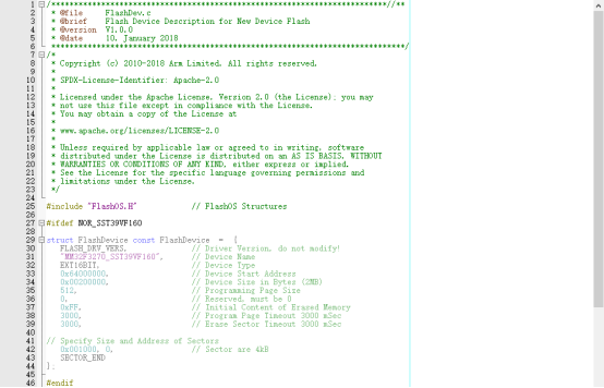
FlashPrg.c is used to implement the interface functions of the programming download algorithm, where some functions must be implemented while others are optional, as shown below:
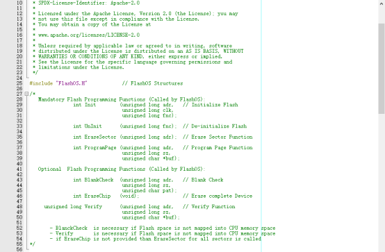
We need to implement these functions to achieve read and write operations on NOR FLASH, allowing us to download programs to NOR FLASH.
In the first section, we know that the download algorithm needs to be loaded into RAM to run before programming operations. The program space size of this download algorithm loaded into RAM actually has a size limit, depending on the RAM size of each chip, but it must not exceed 0x10000.
Therefore, when implementing our defined download algorithm, it is especially important to avoid using library functions, instead using registers or directly manipulating the chip’s internal addresses to save program space as much as possible.
However, this may make the code harder to read and understand. Since the program of the download algorithm cannot be debugged online, it is best to verify the functionality of these functions for NOR FLASH operations in other projects first, confirm that they work correctly, and then port them into the download algorithm project.
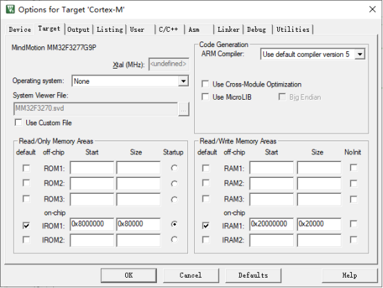
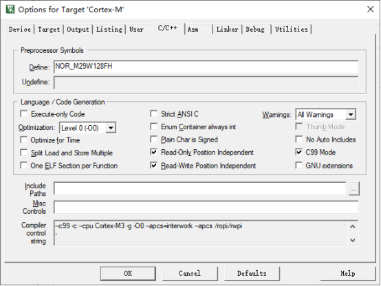
Next, click the KEIL project magic wand button to configure the project. In the Target tab, select the chip model as MM32F3277G9P, and in the C/C++ tab, define macros as needed (since this download algorithm supports multiple NOR FLASH, there are corresponding macro definitions). After adding the relevant functions for NOR FLASH and completing the interface functions, compile the project.
At this time, a FLM file will be generated in the project directory (because there is a command in the User tab: cmd.exe /C copy “Objects\%L” “.\@L.FLM”, which will convert the compiled file into FLM format).
We will copy the generated FLM download algorithm file to C:\Keil_v5\ARM\Flash, and it can be added when needed in future projects.
4. MM32 Implementation of NOR FLASH Application Programming, Downloading Programs, and Running
For programs running in NOR FLASH, there are no special requirements for programming; the only difference is the configuration of the KEIL project. In the example, we only implemented a simple LED blinking function. The KEIL project settings are shown in the figure below:
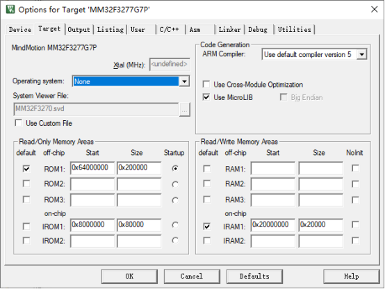
Set the default program space and program startup space to the starting address of NOR FLASH:
Choose the corresponding debugging tool according to the DEBUG tool:

The download tool is the same as the debugging tool:

Select the programming (download) algorithm to be the FLM algorithm generated in the third section, and the corresponding description will be automatically displayed when added:

After completing these configurations, compile and click the download button to download the program to the external storage space of NOR FLASH. Since the RESET AND RUN option is checked, after the download is complete, the MCU will reset, at which point the jump program already exists in the MCU FLASH, which will jump to NOR FLASH to execute the LED blinking program. If the LED light operates normally, it indicates that the program function is running correctly.
Additionally, some may ask why there is an INI file configured in the Utilities tab of the Option for Target window, but I did not include it in my configuration. This INI file contains data that configures the corresponding parameter values for the MCU’s internal address, which is used to set up the MCU before downloading the program. Generally, it configures the FSMC-related registers of the MCU and NOR FLASH to allow the download algorithm to operate NOR FLASH correctly. However, my configuration screenshot does not show this because the INIT function in the download algorithm has already implemented the FSMC initialization configuration, so there is no need to repeat this in the INIT FILE position.
5. Future Work
With this download algorithm, we can direct some programs or data instructions to external storage space. For instance, when displaying image data on an LCD, if the image data is a large array, we can specify this data to NOR FLASH while the application program runs in the internal FLASH of the MCU, as shown in the figure below:
The chip has two ROM spaces, but the default and startup space is the internal FLASH of the MCU:
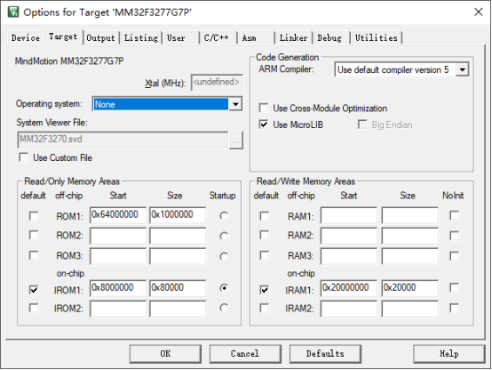
There are two download algorithms, and these two addresses are different: one is for the internal FLASH of the MCU, and the other is for the expanded NOR FLASH:
To specify the program to NOR FLASH, right-click the .C file and select Options for File “IMAGE1.c”…
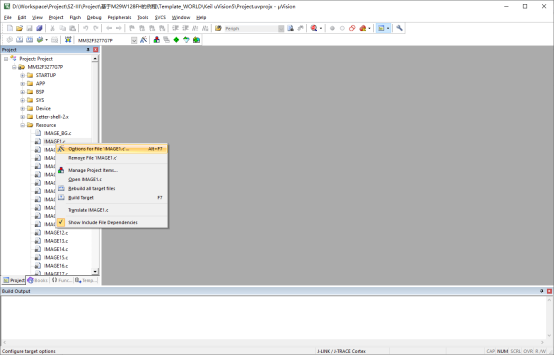
In the popped-up window, direct CODE/CONST to ROM1, as shown in the figure below:
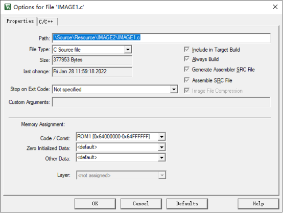
Then, in the program, call the data in the IMAGE1.c file, so when compiling and downloading the program, it will first download the program to the FLASH of the MCU and then download the image data to the expanded NOR FLASH of the MCU.
This article’s hardware is implemented based on the basic Shenzhou III development board, using the MM32F3277G9P from Lingdong Microelectronics and the M29W128FH for NOR FLASH.
Thus, the sharing concludes. I hope it can be helpful to all of you! Additionally, if anyone needs to view the original images and code, please click the bottom “Read the Original” to download.


Add Administrator WeChat