🟩Flash can be divided into two main categories: NOR Flash and NAND Flash. NAND has a large capacity and low cost per unit, while NOR has fast read speeds, high reliability, and quick erase speeds. NOR Flash is primarily used for coding applications, often related to computation; NAND Flash mainly functions as data storage, widely used in embedded systems such as DOCs and flash drives.
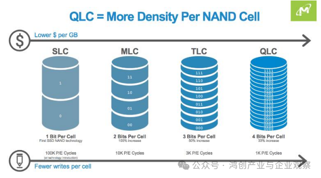
🟧NAND Flash can be divided into four main categories based on the storage density of flash memory chips: SLC, MLC, TLC, and QLC. The main differences between different models lie in cost, capacity, and durability. Capacity depends on the amount of information each cell can store, while durability is determined by the flash memory’s erase/write lifespan (P/E Cycle).
🟪SLC NAND stores 1bit of information per cell, with only two voltage states: 0 and 1, and can endure up to 100,000 write cycles. MLC, TLC, and QLC store increasing amounts of information per cell, but their corresponding P/E lifespans decrease. Compared to SLC, MLC has 100% more capacity but only 1/10 the lifespan. Compared to MLC, TLC has 50% more capacity but only 1/20 the lifespan of SLC.🟥Currently, SLC is used exclusively for enterprise-level server flash memory chips, TLC has become mainstream storage chips, and QLC is the trend for future development. SLC offers the best performance at the highest price, typically used for industrial control, aerospace, military, and communication equipment where reliability, stability, and durability are of utmost importance; MLC is mainstream for industrial-grade and automotive-grade SSD applications; TLC is currently the mainstream for consumer-grade SSDs.
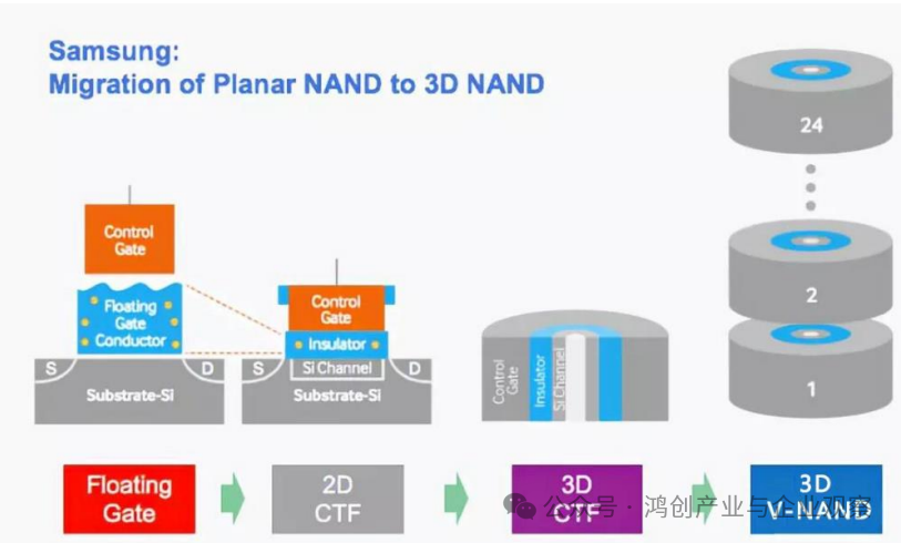
🟦3D NAND addresses the “scaling limitations of flash memory” under 2D structures. 3D NAND refers to the three-dimensional arrangement of storage cells, stacking them vertically in addition to the two-dimensional layout. In 3D NAND, storage cell strings are stretched, folded, and arranged in a U-shaped structure vertically, with cells stacked vertically to increase density. The storage cells in 3D NAND resemble tiny cylindrical structures, with the small cells formed by vertical channels in the middle, where the charge layer is located. By applying voltage, electrons are introduced into the insulating charge storage film and retrieved from it, allowing the signal to be read.
🟫NOR Flash has a small capacity density, slow write and erase speeds, and high costs, but its independent data and address buses provide it with the ability for random access and byte-level programming operations, supporting code execution (Xip), making it extremely suitable for embedded applications. NOR Flash also offers high reliability, fast random read speeds, and longer lifespans.🟨In 2022, the overall market size for storage chips reached $144 billion, with DRAM at $79.7 billion; NAND at $58.7 billion; and NOR at $3.2 billion.Reference: YOLE et al.