ADI, TI’s ADCs, and the ADC from LHA that we looked at yesterday all utilize a Pre-Charge structure at the front end. This means that each conversion of the ADC requires charge to enter the input terminal to establish a steady state. I recently came across an article that discusses this technical detail and found it quite insightful.
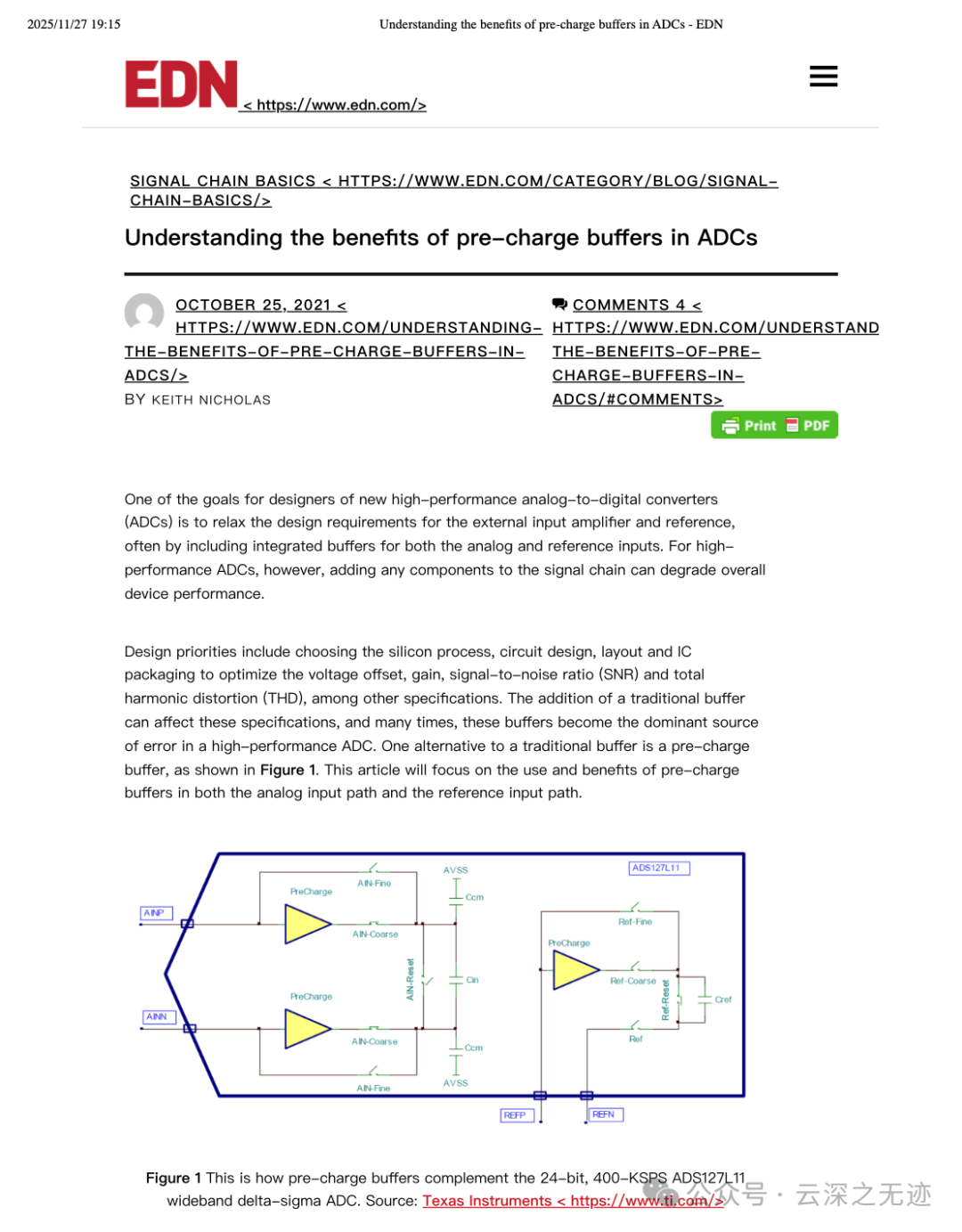
What exactly does the pre-charge buffer do, and why can it significantly reduce the burden on the front-end operational amplifier/reference?
Background: The Power-Hungry Nature of High-Performance ADCs
The front end of high-performance ΔΣ / SAR ADCs essentially consists of a periodic reset + sampling capacitor array: at the start of each sampling, the internal sampling capacitor is “pulled” from 0V to the input voltage.
Abstractly, this means that during each sampling period, a packet of charge is “pumped” into the capacitor.
If this capacitor is charged directly by an external operational amplifier, then:
where is the modulator sampling frequency (equal to half the clock frequency in ADS127L11).
The author first presents the average current formula without any tricks:
This is equation (5): substituting in the result.
Conclusion: The faster the modulation clock, the larger the capacitor, and the higher the amplitude, the greater the average current drawn by the front-end operational amplifier; the peak current is even more exaggerated (tens of mA), which is the main source of THD and power consumption.
Traditional Solution: External “Large Capacitor R-C Charge Bucket”
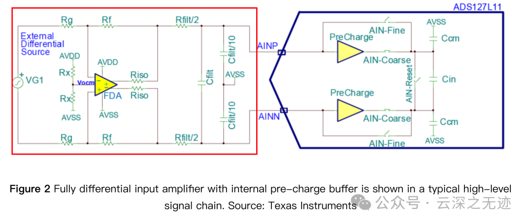
The conventional approach is to connect a pair of relatively large C_filt capacitors to the ADC differential input, along with a resistor, forming a “charge bucket filter” (left half of Figure 2).
Purpose:
C_filt acts as a reservoir, providing the large current during the ADC sampling moment primarily from discharging C_filt, while the operational amplifier is only responsible for slowly charging C_filt — significantly reducing peak current; this allows the use of low-power operational amplifiers with lower bandwidth and weaker driving capability.
However, the problems are also evident: R-C itself is a first-order low-pass filter, severely limiting the maximum input frequency; at high frequencies, the capacitor’s impedance becomes very low, causing large currents to charge and discharge within C_filt, and the operational amplifier still has to supply a large AC current → increasing system power consumption; for signals above 10kHz, if C_filt is chosen too large, the operational amplifier’s power consumption and SNR/THD will deteriorate.
Thus, the large capacitor approach is suitable for ultra-low frequency or DC systems, but not for high-bandwidth ΔΣ like the ADS127L11, which operates at “24bit + 400kSPS”.
The Core Idea of the Pre-Charge Buffer: Rough Charge + Fine Adjustment
The “pre-charge buffer” proposed in the article is the second approach:
Using a dedicated low-power amplifier on-chip, during the first half of the sampling period, it helps to “roughly charge” the internal sampling capacitor to 99.5~99.9% of the target value, and the remaining voltage difference is fine-tuned by the external operational amplifier in the second half.
Structure (Figure 2)
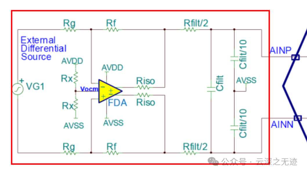
External: differential operational amplifier + appropriate RC filtering;
On-chip: Pre-Charge Buffers: connected between AINP/AINN and the internal sampling capacitor; switch network, AIN-Coarse / AIN-Fine / AIN-Reset three control signals; sampling capacitor:, common-mode capacitor.
The timing in Figure 3 is crucial:
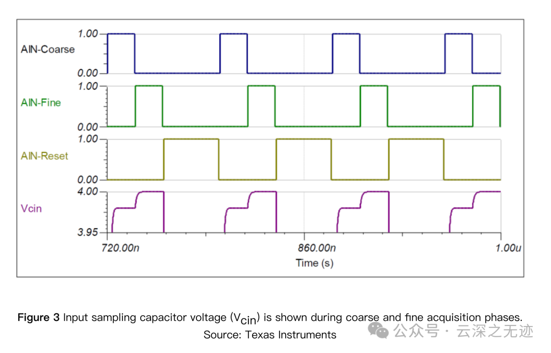
AIN-Reset = 1: internal capacitor discharges to 0, preparing for a new round of sampling;
AIN-Coarse = 1 (rough charge phase): the pre-charge buffer is connected; it charges the to nearly the target voltage, for example, 99.5% of 4.00V → 3.98V; at this point, the external operational amplifier hardly “feels” that capacitor.
AIN-Fine = 1 (fine adjustment phase): the pre-charge buffer is disconnected, and the final fine-tuning is done directly by AINP/AINN to from 3.98V to 4.00V; the key point: at this time, there is no gain/distortion/noise from any buffer in the signal path, equivalent to the traditional sampling capacitor directly connected to the input.
Result: the dynamic large current is handled by the on-chip pre-charge buffer; the external operational amplifier is only responsible for a tiny bit of “finishing up”, with load current << 1% of the original value.
How Does the Average Input Current Decrease? (Formula Derivation)
The article provides a neat and simple derivation.
Without Pre-Charge
As mentioned earlier:
Equation
With Pre-Charge
Assuming the gain of the pre-charge buffer is (ideal value 1, typical for ADS127L11 is 0.995~1.005)
At the end of the rough charge:
The charge stored in the capacitor at this point is:
At the end of the entire sampling, the total charge is still .
Thus, the charge that needs to be supplemented at the external input (Fine phase) is:
Substituting back into the average current formula:
Comparing with the case without pre-charge:
Thus: **the average input current is reduced by a factor of **.
For example, if , then
The external operational amplifier only needs to bear 0.5% of the original average charging current, which means that 99.5% of the “capacitor consumption” work is handed over to the on-chip pre-charge buffer.
How Does the Peak Current Decrease? What Are the Benefits for THD?
For the ADS127L11, the article provides an example: the differential input switch resistance R_sw ≈ 165 Ω.
Peak Without Pre-Charge
If the switch connects from 0V to a 4V signal at the moment of sampling, the peak current is:
For most precision operational amplifiers, this kind of “24mA peak load for each sampling period” is very easy: it pushes the operational amplifier into the nonlinear region, increasing distortion; the output stage power consumption rises, generating heat; requiring high bandwidth and slew rate from the operational amplifier.
Peak With Pre-Charge
If after pre-charging, is already near 3.98V, the Fine phase only needs to adjust from 3.98V to 4.00V:
The peak current drops from 24mA directly to 121µA, a reduction of 200 times.
This way, the external operational amplifier sees a very small burst current, making the operating point more linear; THD can typically improve by over 10dB (the article provides such empirical conclusions); the only downside is that an additional small dynamic amplifier is added on-chip, resulting in a slight increase in total power consumption; however, a lower bandwidth / low power external operational amplifier can offset this.
Reference Pre-Charge Buffer: Driving Multiple ADCs with One Reference
A similar approach is also applied to the reference input.
For example, in the case of ADS127L11:
Without pre-charge: reference voltage 4.096V, high-speed mode, clock 25.6MHz, the average reference current for a single ADC is approximately 778µA.
If creating an 8-channel system, each ADC would require:
Many high-precision references (like REF6041) are rated for a maximum output of 4mA, which cannot support 8 ADCs — an additional high-current buffer amplifier is necessary, which is both expensive and takes up board space, adding noise.

After enabling the reference pre-charge buffer: the average reference input current drops directly to 2µA/ADC; for 8 ADCs, that totals only 16µA, which any precision reference can easily drive, eliminating the need for additional buffers; layout becomes simpler, costs lower, and temperature drift and noise improve.
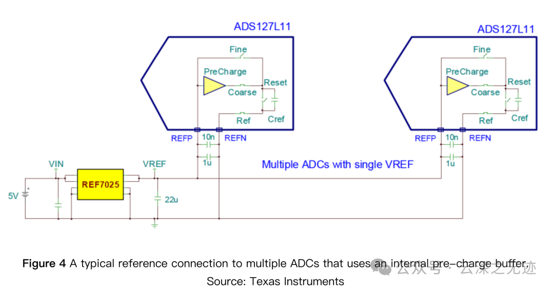
Figure 4 in the article illustrates: a reference chip directly driving multiple ADCs with pre-charge reference buffers.
What Does the Pre-Charge Buffer Really Solve?
Pre-charging (Pre-Charge) is essentially not just about “helping to charge” but rather changing the equivalent “dynamic impedance” of the sampling capacitor, thereby allowing the external operational amplifier to “see” not the capacitor, but a very small residual voltage, making the sampling moment’s dV/dt nearly zero → peak current extremely small → distortion drastically reduced
Next, let’s look at this principle at the device level.
Why Does the Sampling Moment Cause THD? (Fundamental Reason)
The sampling of the ADC is a discontinuous event: the switch transitions from open to closed, instantly connecting the sampling capacitor to the input.
Current at the Sampling Moment:
If the voltage on the sampling capacitor before sampling is , and the input is :
For the ΔΣ modulator, each cycle is “jumping” (due to the internal state of the modulator).
Thus: it is not only large but also non-linear, forcing the input operational amplifier to output tens of mA of peak current, effectively creating an “instant short circuit” load; as a result, the operational amplifier enters a transient nonlinear region; slew rate, input stage, and output stage are all stressed; generating a large number of even and odd harmonics → THD increases.
The core source of THD is the large dV/dt at the sampling moment.
Part 8.2 How Does Pre-Charging Reduce dV/dt to Nearly Zero?
The goal of the pre-charge phase:
Assuming , then:
If , the coarse charge has already charged the capacitor to ±1.995V, and the Fine sampling only needs to supplement 0.02V.
Thus:
Peak Current:
Without Pre-Charge:
With Pre-Charge:
Decay ×200.
The reason for the decay in dV/dt: originally needing to make a “4V transition” now only requires a “0.02V fine adjustment”, which is equivalent to preprocessing the “original jump waveform” into a “small deviation”, leading to a geometric, not linear, improvement in linearity.
Why Does THD Typically Improve by 10–20 dB?
Because THD ≈ operational amplifier non-linearity × impact of ADC sampling, the reduction in peak current by ×100 to ×200 will result in two outcomes:
The Operational Amplifier Remains in the Completely Linear Region
The output stage no longer enters slew rate saturation, and the input differential pair no longer mismatches due to large currents, leading to a significant decrease in THD.
dV/dt is Small → Lower Parasitic Capacitance Injection
One of the largest noise sources at the front end of high-speed ADCs is:charge injection from sampling switches + clock feedthrough, both of which are proportional to dV/dt; after pre-charging, dV/dt is reduced by 200 times → parasitic charge injection from switches is also reduced by 200 times → THD and SFDR improve synchronously.
More Crucially: The Critical Frequency Point (Not Discussed in the Article)
The external operational amplifier does not operate at low frequencies but rather undertakes “dynamic adjustment” near the sampling frequency in the tens of MHz.
Assuming the Fine phase time window is .
Before pre-charging: the input operational amplifier must pull from 0 to the target value within tens of nanoseconds → requiring very high bandwidth & slew rate
After pre-charging:
The input operational amplifier only needs to supplement a very small ΔV, and the required bandwidth is actually:
Typical ΔΣ input:
Resulting in:
This is reasonably achievable.
If there is no pre-charge:
If :
Ordinary high-precision operational amplifiers cannot reach this (they need to be at the level of high-speed video amplifiers).
Why Does Power Consumption Decrease After Enabling Pre-Charge?
Intuitively, adding an on-chip buffer would consume “more power”, but in reality:
The power consumption of the external operational amplifier decreases significantly, thus reducing system power consumption.
Because:
In traditional charging mode: the operational amplifier must output several mA of peak dynamic current each cycle, the internal compensation capacitor is repeatedly excited, and the output stage class-AB is constantly pushed → causing significant fluctuations in supply current, increasing average current.
In pre-charge mode: the external operational amplifier is only responsible for DC + slight AC (a few μA), the bandwidth requirement decreases by an order of magnitude, allowing for a lower power driving amplifier, resulting in very stable supply current.
In many applications: the ADC increases by 1mA, but the external operational amplifier decreases by 8~10mA, resulting in an overall reduction in system power consumption.
From the Noise Perspective: Why Doesn’t Pre-Charge Inject Noise into the Signal Chain?
You might ask:
“Will the on-chip buffer introduce noise into the sampling capacitor?”
The key point is: during the Fine sampling period (the actual sampling moment), the pre-charge buffer is disconnected.
The sampling moment switch topology:
AIN → Rsw → Cin
预充 buffer ——断开
The actual noise during sampling is determined by: the noise of the input operational amplifier, the thermal noise of R_sw (kT/C), Cin + parasitic capacitance distribution, and the internal modulator noise shaping of the ADC.
Therefore:
The pre-charge buffer only works “before sampling” and does not inject any noise during the actual sampling.
This is also why it is called pre-charge rather than input buffer.
When Should Pre-Charge Not Be Used?
The following situations are best to turn off:
Ultra-low frequency / DC measurements (<100 Hz), where external RC is sufficient, dynamic charging is unnecessary, and pre-charging may increase static power consumption; systems with extremely low input signal bandwidth (such as temperature, pressure) where the THD advantage of pre-charging is meaningless; systems that are extremely sensitive to input transients, where even though pre-charge is very small, G ≠ 1 may introduce slight PVT drift (although in ADS127L11, G drift is minimal and nearly negligible).
Simulation
Dynamic Sampling Current Simulation: With / Without Pre-Charge
Simulation Conditions
Sampling Capacitor:
Switch Resistance:
Input Step: 0 → 4 V
Fine Sampling Window: 5 ns
Pre-Charge Gain: (roughly charged to 99.5%)
Using RC charging analytical expressions:
Taking:
Without Pre-Charge:
With Pre-Charge:
Numerical Results
The printed results are:
=== Dynamic Sampling Current: Without Pre-Charge ===
Peak Current I_peak ≈ 24.24 mA
Average Current I_avg ≈ 7.61 mA
Total Charge Q ≈ 38.07 pC

=== Dynamic Sampling Current: With Pre-Charge (G=0.995) ===
Peak Current I_peak ≈ 121.21 µA
Average Current I_avg ≈ 38.07 µA
Total Charge Q ≈ 0.19 pC
Peak Current: 24.2 mA → 0.12 mA (approximately 200 times reduction)
Average Current: 7.6 mA → 38 µA (approximately 200 times reduction)
Total charge also shrinks to about ~0.5%
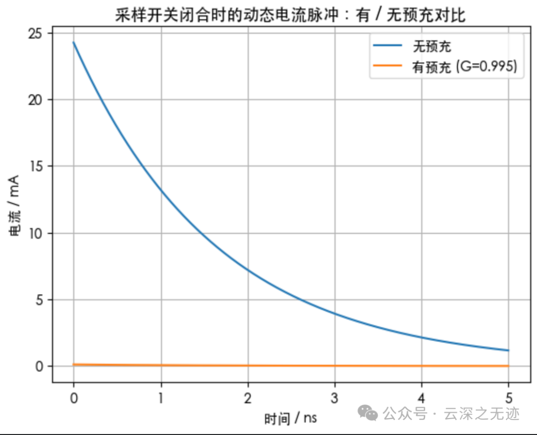
In the figure, you can see:
The blue line (without pre-charge) is a high and sharp exponential decay pulse;
The orange line (with pre-charge) is almost flat near 0, leaving only a very small pulse — this is the intuitive appearance of “no longer drawing large currents at the sampling moment”.
This is completely consistent with our derived formula:
When is, is 0.5%.
FFT Simulation of THD with / without Pre-Charge (Conceptual Model)
Here I created a simplified non-linear model just to visually demonstrate how much THD improves after reducing dynamic current.
Model Settings
Sampling Rate
Input Sine Frequency
Amplitude (close to full scale)
Ideal Sampling Obtained .
Using a 3rd order non-linear model to simulate “distortion of the front-end operational amplifier under heavy load”:
Without Pre-Charge:
With Pre-Charge (current reduced significantly → non-linearity reduced by 10×):
Then applying a Hanning window, performing rFFT, and calculating THD based on the 2nd to 10th harmonics:
Numerical Results
=== THD Simulation Results (Conceptual Model) ===
Without Pre-Charge: THD ≈ -47.8 dB
With Pre-Charge: THD ≈ -67.7 dB
Thus:
Without Pre-Charge: THD ≈ −48 dB
With Pre-Charge: THD ≈ −68 dB → an improvement of nearly 20 dB, which is consistent with the magnitude of “enabling pre-charge/internal buffer improves THD by 10–20 dB” found in many datasheets (this is just a demonstration, not an accurate modeling of a specific ADC).
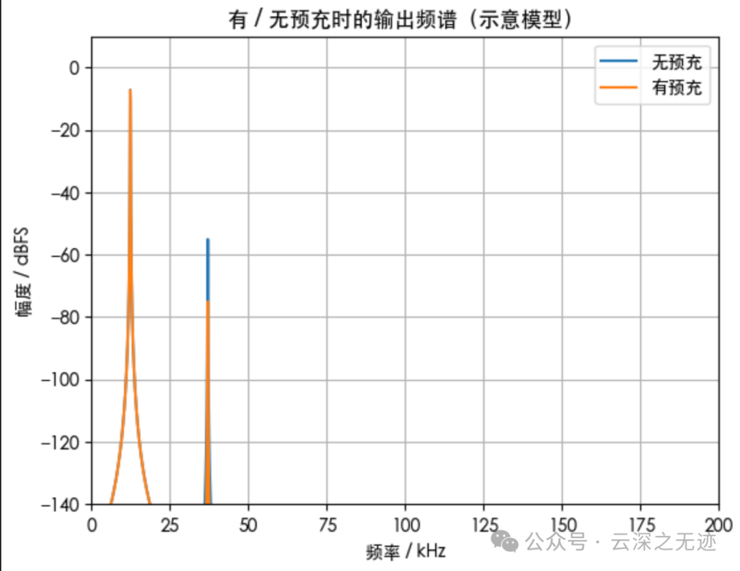
In the spectrum, you can see:
The blue line (without pre-charge): the 2nd, 3rd, and 5th harmonics are quite prominent next to the fundamental;
The orange line (with pre-charge): these harmonics have been significantly reduced overall, and the noise floor is cleaner.
Dynamic Current Simulation Results
Without Pre-Charge: at the moment of sampling, charging a 10 pF capacitor to 4V requires a peak current of approximately 24 mA; with Pre-Charge: only needing to supplement a 0.02V difference, the peak current is approximately 0.12 mA; average current and total charge also shrink proportionally (here about 0.5%).
THD Simulation Results (Toy Model)
Linking the strength of front-end non-linearity with dynamic sampling current, the non-linearity coefficient is reduced by 10×; THD improves by about 20 dB, from −48 dB to −68 dB; the spectrum shows a significant decrease in higher-order harmonics.
How to Use the Information from This Article from an Engineering Perspective?
If Extreme THD / High Bandwidth is Required: Use a high-bandwidth differential driving amplifier + enable the ADC’s pre-charge buffer; the operational amplifier bandwidth requirement can be reduced to <10MHz, but the system THD can still be about 10dB better than “operational amplifier direct drive + large capacitor”.
If Designing a Multi-Channel System (e.g., 8× ADS127L11): It is strongly recommended to enable the reference pre-charge buffer, allowing a high-precision reference to directly drive all channels, eliminating the need for multiple reference buffers.
If Input Frequencies Are Very Low (Within a Few Hundred Hz): You can also forgo pre-charge, using simple RC + slow operational amplifiers; however, with the option of pre-charge, you can make trade-offs at the system level based on power consumption / bandwidth / THD.
From a Modeling Perspective, Remember:
Without Pre-Charge:
With Pre-Charge:, the peak current is also reduced to the same order of magnitude; when G≈0.995, “the external operational amplifier only bears 0.5% of the dynamic charging”.
The essence of pre-charging is:
To spread the “large jump at the moment of sampling” into “two stages: rough charge + fine adjustment”, allowing the dV/dt at the actual sampling moment to become extremely small, enabling the external operational amplifier to enter the “completely linear region”, thereby reducing THD (10–20 dB), reducing peak current (×100 to ×200), and lowering power consumption.
This is one of the most elegant solutions to the classic SAR/ΔΣ input driving problem.
import numpy as np
import matplotlib.pyplot as plt

# ==============================
# ① Dynamic Sampling Current Simulation: With / Without Pre-Charge
# ==============================

# Parameter Settings
Cin = 10e-12      # Sampling Capacitor 10 pF
Rsw = 165.0       # Switch Equivalent Resistance 165 Ω
Vin = 4.0         # Input Step 0 -> 4 V
G_pre = 0.995     # Pre-Charge Gain (roughly charged to 99.5%)
Tfine = 5e-9      # Fine Sampling Window 5 ns
dt = 5e-12        # Simulation Time Step 5 ps

t = np.arange(0, Tfine, dt)

def current_pulse(V_init):
    """
    Given the initial voltage V_init on the capacitor at the start of sampling,
    calculate the current i(t) through Rsw during the Fine sampling phase.
    Assume the input remains Vin, and the switch closes to form RC charging.
    """
    tau = Rsw * Cin
    dVdt = (Vin - V_init) * np.exp(-t/tau) / tau
    i = Cin * dVdt
    return i

# Case A: Without Pre-Charge, V_init = 0
i_no_pre = current_pulse(0.0)

# Case B: With Pre-Charge, V_init = G_pre * Vin
i_pre = current_pulse(G_pre * Vin)

def pulse_metrics(i, dt):
    I_peak = np.max(i)
    Q = np.trapz(i, dx=dt)
    I_avg = Q / (t[-1] - t[0])
    return I_peak, I_avg, Q

Ipk_no, Iavg_no, Q_no = pulse_metrics(i_no_pre, dt)
Ipk_pre, Iavg_pre, Q_pre = pulse_metrics(i_pre, dt)

print("=== Dynamic Sampling Current: Without Pre-Charge ===")
print(f"Peak Current I_peak ≈ {Ipk_no*1e3:.2f} mA")
print(f"Average Current I_avg ≈ {Iavg_no*1e3:.2f} mA")
print(f"Total Charge Q ≈ {Q_no*1e12:.2f} pC")
print()
print("=== Dynamic Sampling Current: With Pre-Charge (G=0.995) ===")
print(f"Peak Current I_peak ≈ {Ipk_pre*1e6:.2f} µA")
print(f"Average Current I_avg ≈ {Iavg_pre*1e6:.2f} µA")
print(f"Total Charge Q ≈ {Q_pre*1e12:.2f} pC")

# Plot Current Pulse Waveform
plt.figure()
plt.plot(t*1e9, i_no_pre*1e3, label="Without Pre-Charge")
plt.plot(t*1e9, i_pre*1e3, label="With Pre-Charge (G=0.995)")
plt.xlabel("Time / ns")
plt.ylabel("Current / mA")
plt.title("Dynamic Current Pulse at Sampling Switch Closure: Comparison With / Without Pre-Charge")
plt.legend()
plt.grid(True)

# ==============================
# ② THD FFT Simulation With / Without Pre-Charge
# ==============================

Fs = 1_000_000.0       # 1 MS/s Sampling Rate
fin = 12345.0          # Input Sine Frequency
A = 0.9                # Amplitude
N = 2**14
n = np.arange(N)
t_s = n / Fs

x = A * np.sin(2 * np.pi * fin * t_s)

# Conceptual Non-Linear Model
a3_no_pre = 0.02
a3_pre = 0.002  # Reduced by 10 times

y_no_pre = x + a3_no_pre * x**3
y_pre = x + a3_pre * x**3

def compute_thd_db(y, Fs, fin):
    w = np.hanning(len(y))
    yw = y * w
    Y = np.fft.rfft(yw)
    mag = np.abs(Y) / (len(y)/2)
    freqs = np.fft.rfftfreq(len(y), d=1/Fs)

    k1 = np.argmin(np.abs(freqs - fin))
    A1 = mag[k1]

    harmonics = []
    for k in range(2, 11):
        fk = k * fin
        if fk > Fs/2:
            break
        idx = np.argmin(np.abs(freqs - fk))
        harmonics.append(mag[idx])
    A_h = np.sqrt(np.sum(np.array(harmonics)**2))

    thd = A_h / A1
    thd_db = 20 * np.log10(thd + 1e-15)
    return thd_db, freqs, 20*np.log10(mag + 1e-15)

thd_no, f_no, spec_no = compute_thd_db(y_no_pre, Fs, fin)
thd_pre, f_pre, spec_pre = compute_thd_db(y_pre, Fs, fin)

print("\n=== THD Simulation Results (Conceptual Model) ===")
print(f"Without Pre-Charge: THD ≈ {thd_no:.1f} dB")
print(f"With Pre-Charge: THD ≈ {thd_pre:.1f} dB")

plt.figure()
plt.plot(f_no/1e3, spec_no, label="Without Pre-Charge")
plt.plot(f_pre/1e3, spec_pre, label="With Pre-Charge")
plt.xlim(0, 200e3/1e3)
plt.ylim(-140, 10)
plt.xlabel("Frequency / kHz")
plt.ylabel("Magnitude / dBFS")
plt.title("Output Spectrum With / Without Pre-Charge (Conceptual Model)")
plt.legend()
plt.grid(True)
plt.show()