The most basic purpose of PCB surface treatment is to ensure good solderability or electrical performance.Since copper in nature tends to exist in the form of oxides in the air, it is unlikely to remain as pure copper for a long time, so additional treatments are required for copper.There are now many PCB surface treatment processes, the most common being Hot Air Leveling, Organic Solderability Preservatives (OSP), Nickel-Gold Plating, Gold Immersion, Tin Immersion, Silver Immersion, Chemical Nickel Palladium Gold, and Electroplated Hard Gold.
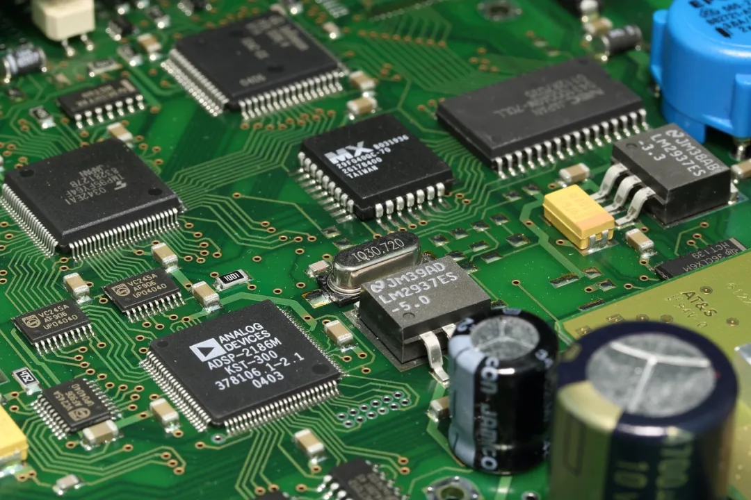 1. Hot Air Leveling (HASL) The general process of hot air leveling is: Micro-etching → Preheating → Coating flux → Hot air leveling → Cleaning. Hot air leveling, also known as hot air solder leveling, is a process where molten solder (tin-lead) is coated on the PCB surface and leveled using heated compressed air, forming a layer that resists copper oxidation and provides good solderability. During hot air leveling, a copper-tin intermetallic compound forms at the junction of solder and copper. The PCB must be submerged in molten solder during hot air leveling; the air knife levels the liquid solder before it solidifies; the air knife minimizes the meniscus of solder on the copper surface and prevents solder bridging. Hot air leveling can be vertical or horizontal, with horizontal being generally preferred due to its more uniform coating, allowing for automated production. Advantages: Longer storage time; After completion, the copper surface is fully wetted (completely covered with tin before soldering); Suitable for lead-free soldering; Mature process, low cost, suitable for visual inspection and electrical testing. Disadvantages: Not suitable for wire bonding; due to surface flatness issues, there are limitations in SMT; not suitable for contact switch designs. During hot air leveling, copper will dissolve, and the board undergoes high temperatures once. Very thick or thin boards have limitations with hot air leveling, making production operations inconvenient.2. Organic Solderability Preservatives (OSP) The general process is: Degreasing → Micro-etching → Acid washing → Pure water cleaning → Organic coating → Cleaning, process control is relatively easier compared to other surface treatment processes. OSP is a process that meets the requirements of the RoHS directive for copper foil surface treatment in printed circuit boards (PCBs). OSP stands for Organic Solderability Preservatives, which translates to organic solder mask, also known as copper protector, and is also referred to as Preflux in English. In simple terms, OSP is a chemical method of growing a layer of organic film on a clean bare copper surface. This film provides oxidation resistance, thermal shock resistance, and moisture resistance, protecting the copper surface from further rusting (oxidation or sulfuration, etc.) in normal environments; however, during subsequent soldering at high temperatures, this protective film must be easily removed by flux so that the exposed clean copper surface can quickly bond with molten solder to form a strong solder joint. Advantages: Simple process, very flat surface, suitable for lead-free soldering and SMT. Easy to rework, convenient for production operations, suitable for horizontal line operations. Multiple treatments can coexist on the board (e.g., OSP + ENIG). Low cost, environmentally friendly. Disadvantages: Limitations on the number of reflow soldering (multiple thick soldering can damage the film, generally no problem with 2 times). Not suitable for press-fit technology or wire bonding. Visual inspection and electrical testing are inconvenient. Requires N2 gas protection during SMT. SMT rework is not suitable. High storage condition requirements.3. Full Board Nickel-Gold Plating Nickel-gold plating involves first plating a layer of nickel on the PCB surface conductors followed by a layer of gold, with nickel primarily serving to prevent diffusion between gold and copper. Current nickel-gold plating has two types: Soft gold (pure gold, the gold surface appears dull) and hard gold (smooth and hard surface, wear-resistant, containing cobalt and other elements, the gold surface appears brighter). Soft gold is mainly used for bonding gold wires during chip packaging; hard gold is mainly used for electrical interconnections in non-soldering areas. Advantages: Longer storage time > 12 months. Suitable for contact switch design and wire bonding. Suitable for electrical testing. Disadvantages: Higher cost due to thicker gold. Additional design lines are needed for conductive gold fingers. Due to inconsistent gold thickness, it may lead to solder joint embrittlement and affect strength when used in soldering. Issues with the uniformity of the electroplated surface. The nickel-gold plating does not cover the edges of the wires. Not suitable for aluminum wire bonding.4. Gold Immersion The general process is: Acid wash cleaning → Micro-etching → Pre-soaking → Activation → Chemical nickel plating → Chemical gold immersion; this process involves six chemical tanks and nearly a hundred types of chemicals, making it relatively complex. Gold immersion wraps a thick layer of electrically conductive nickel-gold alloy on the copper surface, which can protect the PCB for a long time; additionally, it has environmental resistance that other surface treatment processes do not possess. Moreover, gold immersion can prevent copper dissolution, which benefits lead-free assembly. Advantages: Not easy to oxidize, can be stored for a long time, flat surface, suitable for soldering fine-pitch pins and small solder joints. Preferred for button PCB boards (e.g., mobile phone boards). Can undergo multiple reflow solderings without significantly reducing solderability. Can be used as a substrate for COB (Chip On Board) wire bonding. Disadvantages: Higher cost, poorer solder joint strength due to the use of non-electroplated nickel processes, prone to black pad issues. The nickel layer will oxidize over time, raising long-term reliability concerns.5. Tin Immersion Since all current solder materials are based on tin, the tin layer can match any type of solder. Tin immersion can form a flat copper-tin intermetallic compound, which gives it good solderability similar to hot air leveling without the flatness issues that hot air leveling presents; however, tin immersion boards cannot be stored for too long and must be assembled based on the sequence of tin immersion. Advantages: Suitable for horizontal line production. Suitable for fine line processing, lead-free soldering, especially suitable for press-fit technology. Excellent flatness, suitable for SMT. Disadvantages: Requires good storage conditions, preferably not exceeding 6 months, to control tin whisker growth. Not suitable for contact switch designs. The production process has high requirements for the solder mask process; otherwise, it may lead to solder mask peeling. Multiple solderings require N2 gas protection. Electrical testing is also a concern.6. Silver Immersion Silver immersion is a process that lies between organic coating and chemical nickel/gold immersion, with a relatively simple and fast process; even when exposed to heat, moisture, and polluted environments, silver can still maintain good solderability, although it will lose its luster. Silver immersion does not have the good physical strength that chemical nickel/gold immersion possesses because there is no nickel beneath the silver layer. Advantages: Simple process, suitable for lead-free soldering and SMT. Very flat surface, low cost, suitable for very fine lines. Disadvantages: High storage condition requirements, easily contaminated. Solder joint strength can easily become an issue (micro-void issues). Prone to electromigration and the phenomenon of Giovanni etching under the solder mask copper. Electrical testing is also a concern.7. Chemical Nickel Palladium Gold Chemical nickel palladium gold has an additional layer of palladium between nickel and gold compared to gold immersion, which can prevent corrosion caused by replacement reactions, thus adequately preparing for gold immersion. Gold tightly covers the palladium, providing a good contact surface. Advantages: Suitable for lead-free soldering. Very flat surface, suitable for SMT. Through-holes can also be coated with nickel-gold. Longer storage time, storage conditions are not strict. Suitable for electrical testing. Suitable for switch contact design. Suitable for aluminum wire bonding, suitable for thick boards, strong against environmental attacks.8. Electroplated Hard Gold Hard gold plating is used to enhance product wear resistance and increase plug-in cycles. The changes in PCB surface treatment processes are not significant, and seem quite distant, but it should be noted that: Long-term gradual changes will lead to significant transformations. In the context of increasing environmental protection calls, the surface treatment processes of PCBs will undoubtedly undergo significant changes in the future.
Source: Baineng
Statement: This article’s copyright belongs to the original author and does not represent the association’s views. Articles pushed by the “Jiangxi Province Electronic Circuit Industry Association” are for sharing purposes only and do not represent this account’s stance. If there are copyright issues, please contact us for removal.