RZ/T2H
This article discusses the RZ/T2H’s PCIe peripheral functioning as an Endpoint (EP) and the potential issues that may arise when developing drivers and conducting speed tests on Windows, particularly the problem of Windows not recognizing the device. It summarizes various debugging methods and techniques to identify and resolve these issues.
As shown in the figure below, the RZ/T2H has a rich set of peripheral resources.
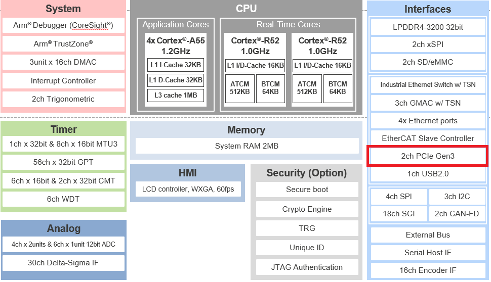
Figure 1: RZ/T2H System Block Diagram
As indicated in the red box, the RZ/T2H features two third-generation PCIe interfaces, supporting a maximum transfer rate of up to 8.0 GT/s. The physical connection can be configured as x1 or x2, and both interfaces can independently function as Root Complex (RC) and Endpoint (EP).
In a certain integrated control project, the customer used one PCIe interface as an EP, configured as x1; a Windows PC served as the RC, enabling fast communication via PCIe. We developed the relevant driver on the Windows side based on the Windows Driver Framework.
Considering that Windows is a non-real-time operating system, all code interacting with PCIe was placed in the driver layer to enhance communication real-time performance. Testing showed that with the Windows PC as the RC and the RZ/T2H as the EP, the data transfer rate for the RC reading data was: 33 Bytes/us (given that Windows is a non-real-time operating system, it is normal that the transfer rate does not reach 8GT/s). If the T2H Evaluation Kit (EVK) is used as the RC side, the rate can reach the PCIe 3.0 standard.
The PCIe 3.0 standard specifies a transfer rate of 8.0 GT/s. According to the 128b/130b encoding rule, the effective data rate is calculated as 8.0 × 0.9846 = 7.877 Gbit/s ≈ 0.985 GB/s per lane, or 985 bytes/us.
The default Maximum Payload Size (MPS) for T2H can be configured up to 4096B. Considering the addition of the TLP header (assuming 3WD, 12B, and MPS configured to 256B), the effective data transfer amount is (RC continuously sends MRd).
1
The number of complete completions that can be transmitted per us is: 985/(256+12) ≈ 3.67 times
2
The corresponding effective data amount is approximately 3.67 × 256 ≈ 939B/µs
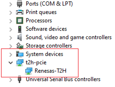
Figure 2: RZ/T2H Driver Program
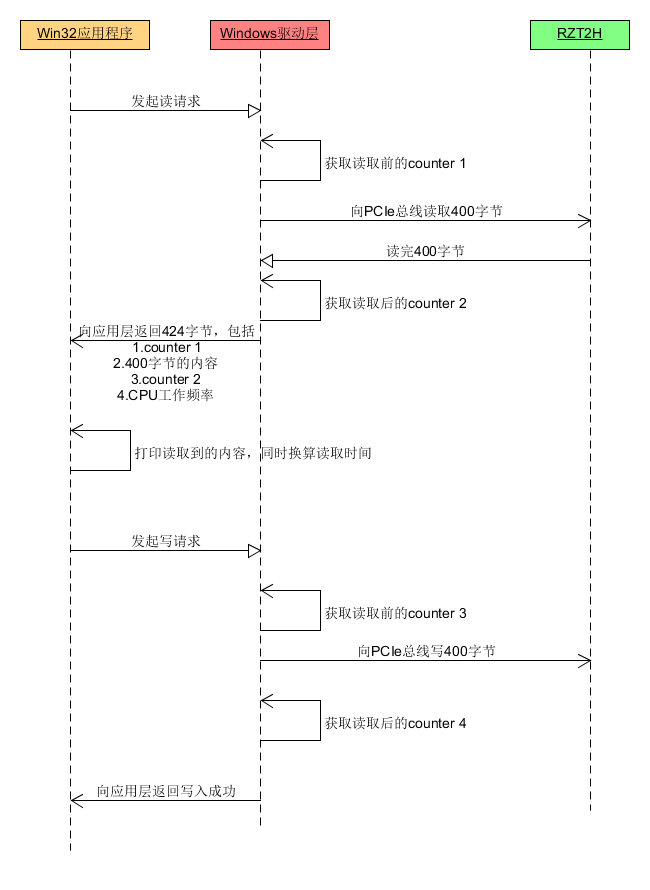
Figure 3: Message Sequence Diagram for Measuring PCIe Read/Write Rates on Windows
The customer’s motherboard design connects to the PCIe x1 interface of the PC motherboard via PCIe gold fingers. The issue encountered was that after programming the customer’s motherboard and connecting it to the PC, it was not recognized by the PC.
Due to the lack of a high-speed oscilloscope to analyze anomalies on the PCIe bus, we could only analyze from the following perspectives.
1
Check if the power supply is reasonable.
We checked 5V, 3.3V, 1.8V, and 0.8V sequentially, all of which were normal.
2
With only a 500M oscilloscope, we could only capture the startup waveform. We compared the waveforms from the RZ/T2H EVK with those from the customer’s board.
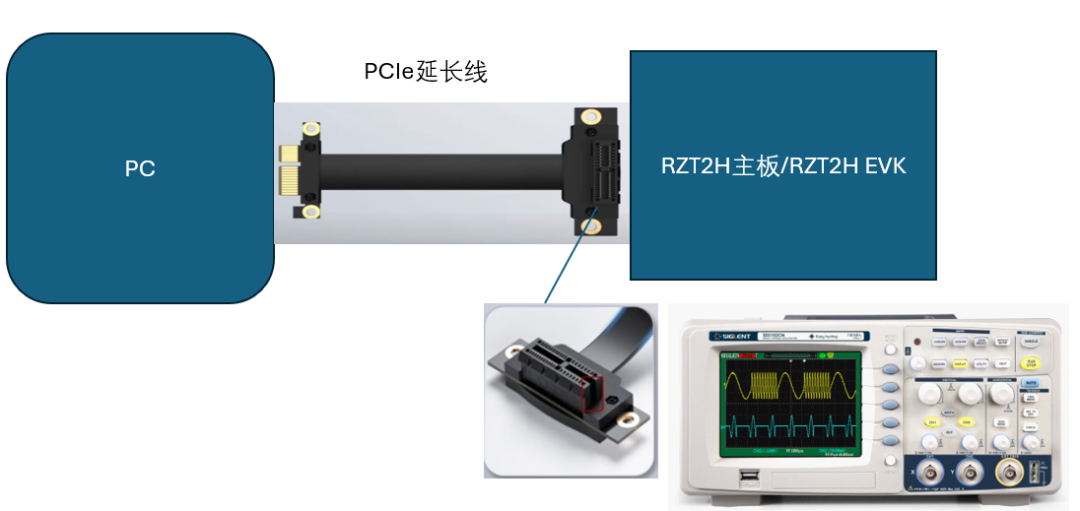
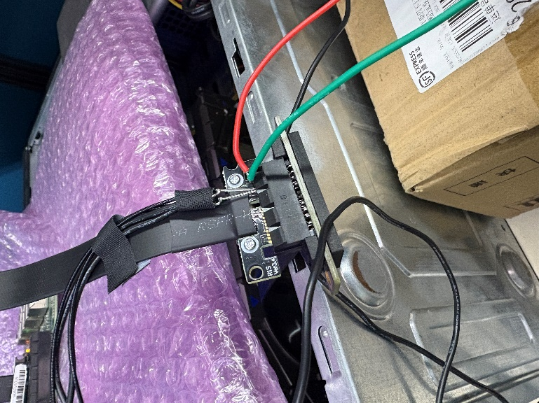
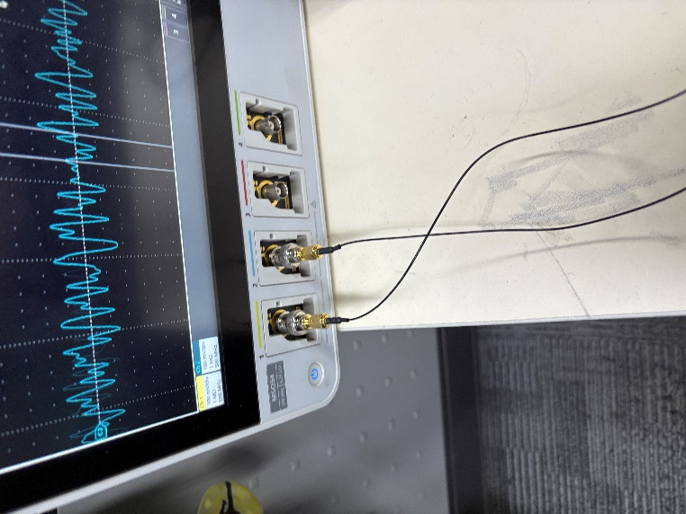
Figure 4: Using PCIe Extension Cable to Capture Necessary Waveforms
Through the PCIe startup process, we learned that when the link has not yet been trained (LTSSM has not entered the L0 normal operating state), devices are allowed to notify each other of their presence. This notification is defined as a Beacon, which is a low-speed, low-frequency physical signal, not a PCIe 8b/10b or 128b/130b encoded data stream.
In light of this, we used a 500M oscilloscope to connect TX+ (B14) and TX- (B15) through the PCIe extension cable to the oscilloscope. C1 is TX+, and C2 is TX-.
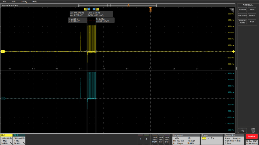
Figure 5: RZ/T2H EVK Beacon
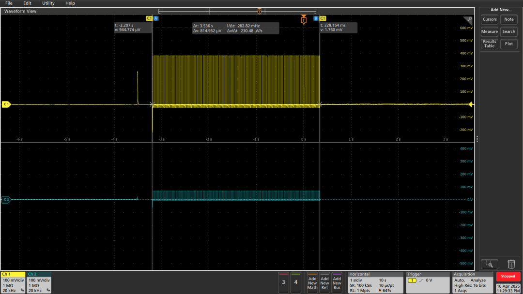
Figure 6: Customer RZ/T2H Motherboard Beacon
From Figures 5 and 6, we can see:
-
The RZ/T2H EVK’s Beacon duration is 370ms, with TX+ and TX- amplitudes around 400mV, and they are very symmetrical.
-
The customer’s RZ/T2H motherboard’s Beacon duration is 3.5s, suggesting that the reason for the prolonged Beacon duration is the lack of response from the EP. Additionally, the amplitude of TX+ is around 400mV, while that of TX- is less than 100mV, indicating asymmetry.
TX+/TX- is a signal initiated from the RC side; why does the waveform exhibit asymmetry at the gold finger end? We carefully checked the customer’s PCB and found that layers 6 and 7 did not have a ground plane.
Due to local differences between the customer’s circuit and the EVK, to avoid misjudgment, we modified the RZ/T2H EVK to match the customer’s board configuration (resistor values and corresponding signal floating, etc.), and the development board was able to start PCIe normally, indicating that the lack of a ground plane on the PCB likely caused the differential signal imbalance, preventing the RZ/T2H from correctly receiving the handshake signal from the PC as an EP, thus not responding to the RC and halting further actions.
After the customer re-laid the board, the motherboard was able to perform normal PCIe communication.
This debugging process highlights the critical importance of PCIe reference ground. If PCIe signal lines are routed without a reference ground plane, it can lead to issues such as:
1
Impedance discontinuity and severe reflections: Impedance fluctuates dramatically along the trace, causing reflections at each point of impedance change. This severely degrades signal quality. If the ground plane is broken or split, it can lead to local impedance jumps, increasing reflections and potentially causing link training failures.
2
Signal Integrity (SI) Issues:
-
Eye diagram collapse: The eye diagram observed at the receiver will appear very “thin” or even completely closed, with both eye height and width failing to meet standards.
-
Ringing and overshoot/undershoot: Due to impedance mismatch and reflections, signals can exhibit severe oscillations.
-
Timing errors: Edges become slow and uncertain, and setup and hold times cannot be met.
3
Electromagnetic Interference (EMI) Issues: The lack of a reference plane means that the electromagnetic fields generated by the signals cannot be effectively shielded and contained, leading to radiation and potential EMI test failures, which may also interfere with other circuits on the board.
4
System instability and high error rates: The end result is PCIe link training failures, inability to negotiate rates, or a high incidence of data errors (BER spikes), leading to frequent blue screens, stuttering, and device recognition failures.
For PCIe 3.0 and above rates, layout requirements are stringent. PCB designers must take this seriously; without a complete reference ground plane, the risk of project failure is extremely high, which will also lead to unnecessary debugging work later. The PCB must adhere to the RZ/T2H hardware design guidelines.
For complete software and hardware design specifications, reference examples, tools, etc., please visit the following URL for more information:

https://www.renesas.com/en/products/rz-t2h

Need Technical Support?
If you have any questions while using Renesas MCU/MPU products, you can scan the QR code below or copy the URL into your browser to access theRenesas Technical Forum for answers or online technical support.

https://community-ja.renesas.com/zh/forums-groups/mcu-mpu/
1
END
1
Recommended Reading

Video Tutorial | RZ/T2H – Achieving Inter-Core Communication
New Benchmark for Industrial MPU, Multi-Protocol Industrial Ethernet + Motion Control – Renesas RZ/T2H New Product Mass Production Launch

New Choice of Industrial Microprocessor Supporting EtherCAT Protocol – Review of Renesas RZ/T2L Evaluation Kit (Software Edition)