1. Overview
Traditional two-wire communication typically operates at a baud rate of 9600 bps. For high-speed communication applications, where the bus bandwidth needs to reach 115200 bps or even 1 Mbps, it can be specially customized based on the actual project requirements.
2. HS2485 Development Board Parameters
Since communication and power are combined into two wires, it means that the power supply and load will introduce different interferences to the communication. It is necessary to provide the bus power supply voltage, the number of nodes, the current consumption of different nodes, communication distance, and load types (such as screens, relays, motors, etc.) to customize specific modules, enabling high-speed serial transparent transmission functions with a baud rate of <1 Mbps.
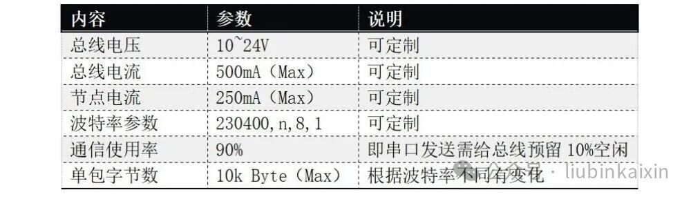
The demo board is designed with the following parameters. If the baud rate interface is below 230400 bps, it can be tested directly with the demo board. For high-speed communication two-wire systems, the distance is generally not too far, typically within a few meters to several tens of meters. The higher the baud rate, the closer the distance, so it should primarily meet the application of your product.
Table 1 HS2485 Demo Board Parameters
3. Port Description
The HS2485 module is powered by 3.3V and includes half-duplex and full-duplex serial ports and an RST reset pin (active low). The bus interface BUS+ and BUS- are directly connected to the bus, and the size of the HS2485 module varies based on actual customization.
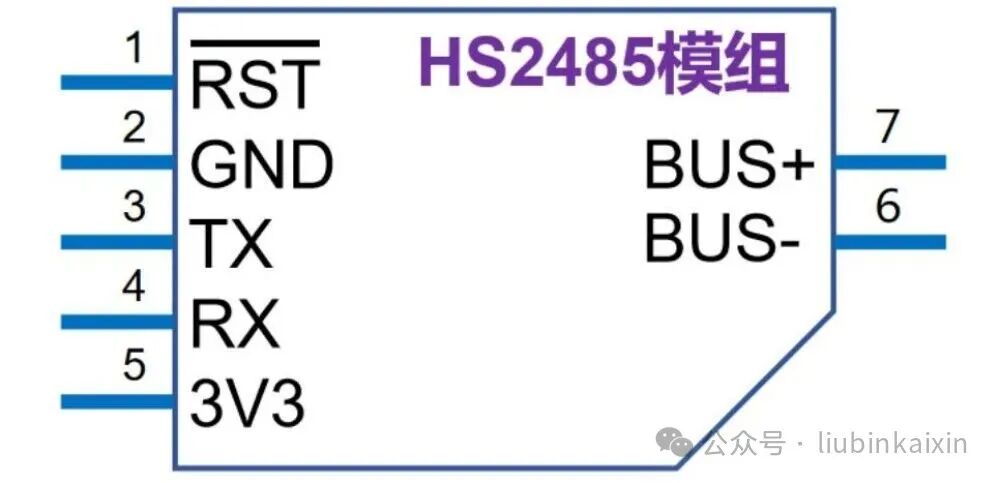
Figure 1 HS2485 Port Schematic
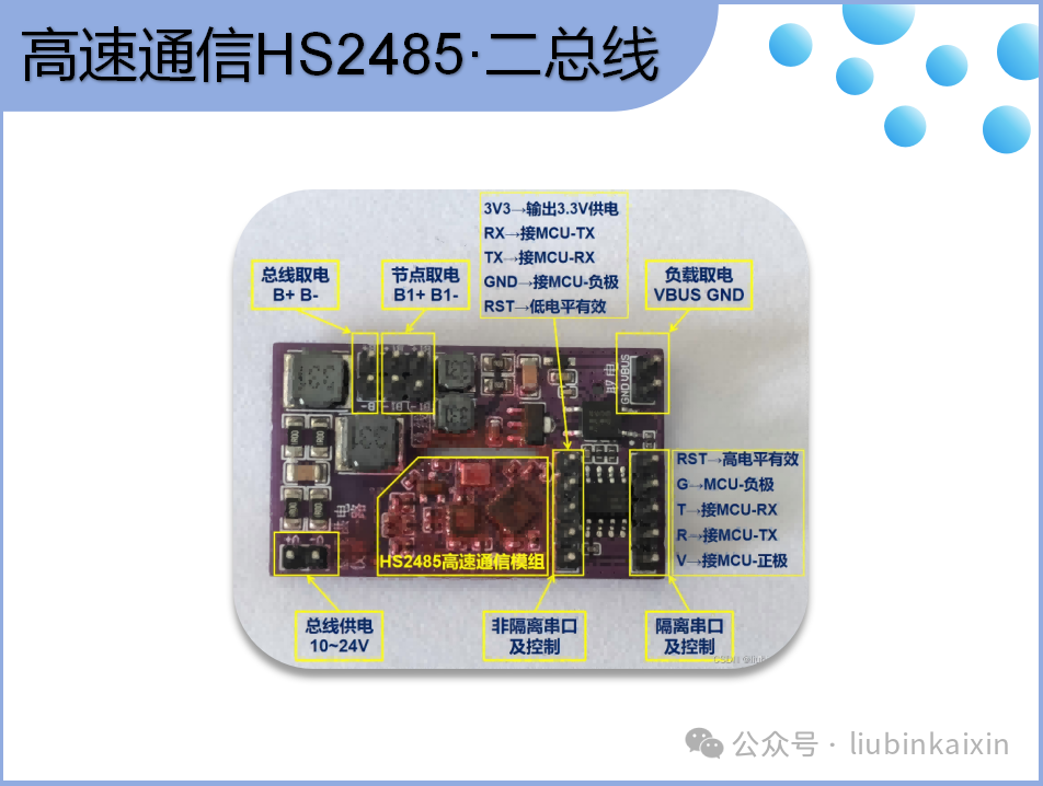
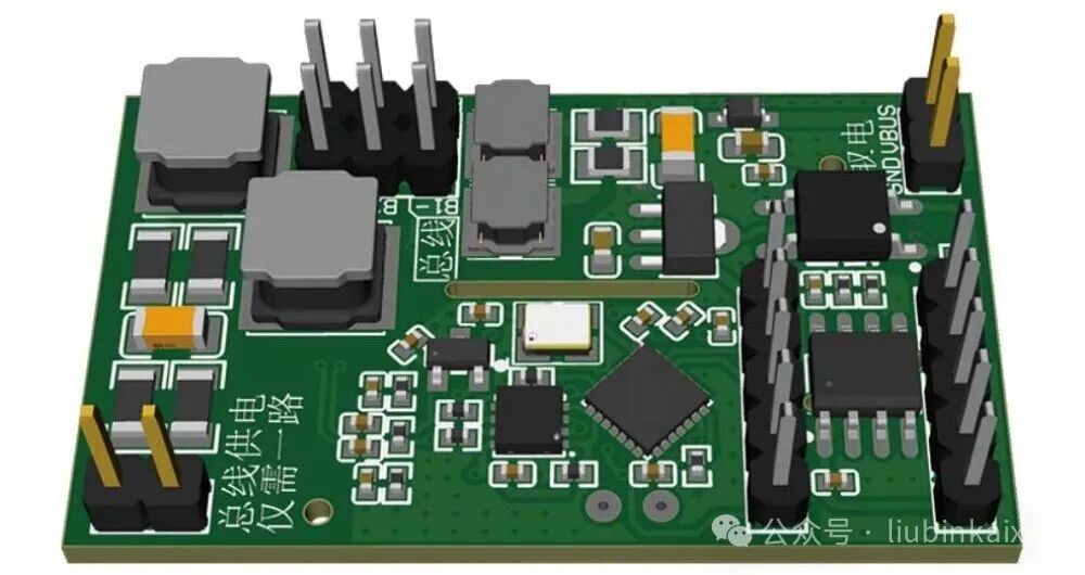
The HS2485 development board consists of bus power supply, slave power extraction, HS2485 high-speed communication module, and isolated serial port. In system design, it is recommended that your product’s host use isolated serial communication, and the host should draw power directly from the power supply; the slave device should draw power from the bus, communicate through a non-isolated port, and supply power to the load through VBUS and GND. Refer to the next section for specific wiring.
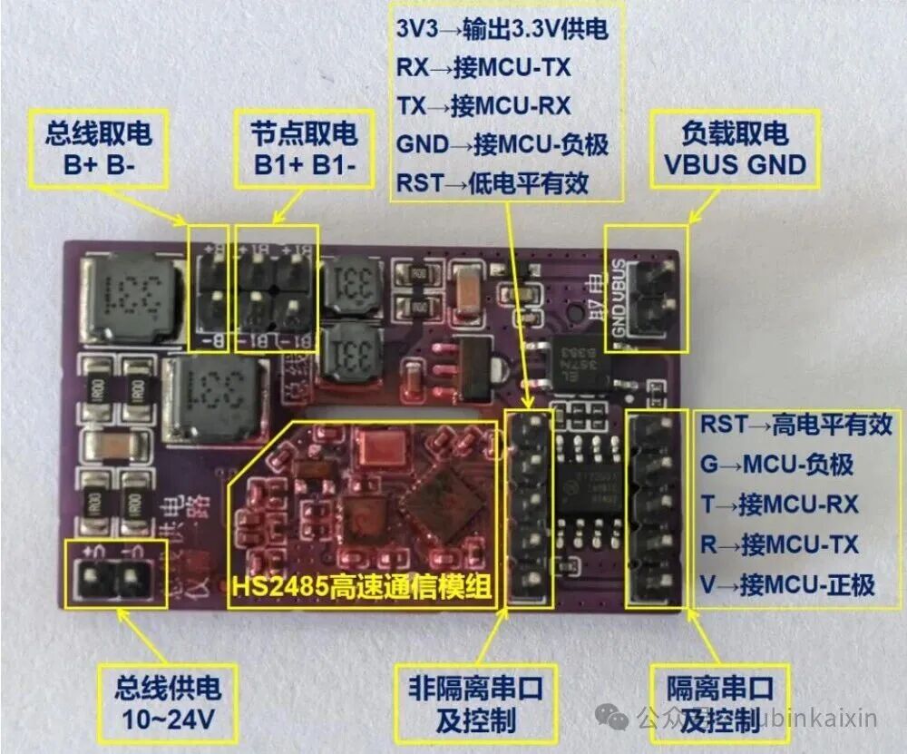
Figure 2 HS2485 Development Board Port and Usage Introduction
4. Wiring Instructions
The wiring diagram for the HS2485 module host and slave is shown below. Pay attention to the power supply and bus polarity; do not connect them incorrectly!
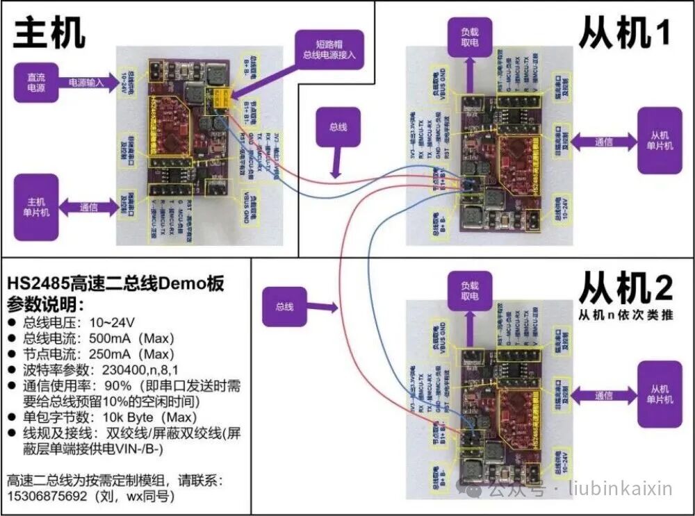
Figure 3 HS2485 Development Board Wiring Diagram
5. HS2485 Peripheral Design Description
The HS2485 peripherals mainly include bus power supply, bus power extraction, and isolated communication, where the power supply and bus, as well as the bus and load, are isolated by a 330uH inductor. The inductor value may need to be adjusted according to different baud rates.
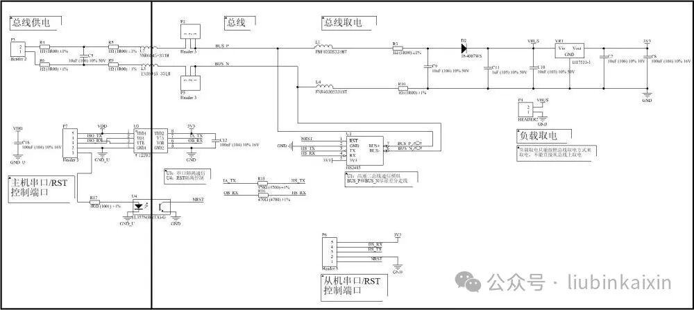
Figure 4 HS2485 Peripheral Design Schematic