In the previous article, I documented how I used the STM32F103 to light up the ILI9341 LCD using the SPI protocol. This time, we plan to use the same microcontroller to drive the OV7670 camera and display it on the LCD, but ultimately we did not fully succeed. The camera test pattern can be displayed correctly, but the image still does not show up. Below are the records of the experiment, and I hope everyone can provide some guidance.Hardware ConnectionsThe camera module is as follows: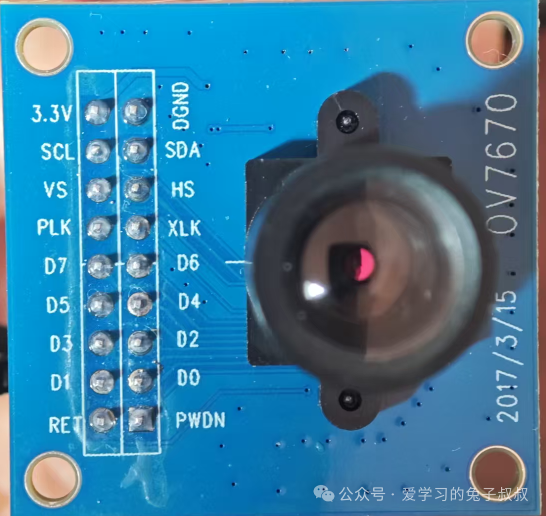 Connections to the STM32 are as follows:
- 3.3V, GND, connected to the corresponding 3.3V and GND
- SCL, SDA: Clock and data pins for the SCCB protocol. Since the two-wire SCCB protocol is fully compatible with the I2C protocol, we can use the STM32’s I2C functionality for direct communication. Here we use I2C2 of the F103, connecting SCL to PB10 and SDA to PB11, enabling I2C2 in CubeMX. The speed mode is standard, with an I2C clock of 100kHz. Additionally, the I2C pins need pull-up resistors, so both pins are connected with 4.7k pull-up resistors.
- VS, HS: Frame synchronization and horizontal synchronization signals, connected to PC11 and PC10, set as GPIO Input.
- PLK: Pixel clock signal, active on the rising edge, connected to PC12, set as GPIO Input.
- XLK: Camera clock. The recommended clock range for the OV7670 is 10MHz to 48MHz, with a typical value of 24MHz. However, since we plan to use GPIO pins to directly collect data, the performance of GPIO pins is limited, so we need to reduce the clock frequency as much as possible. Here we directly use the RCC_MCO of pin PA8 and select the MCO clock source as HSE, which is 8MHz.
- D7~D0: These are the output pins of the camera, connected to PC7~PC0, all set as GPIO Input.
- RET: Reset pin, low level resets, high level operates normally. To simplify wiring, it is directly connected to 3.3V.
- PWDN: Power-down mode, low level operates normally, high level saves power. To simplify wiring, it is directly grounded.
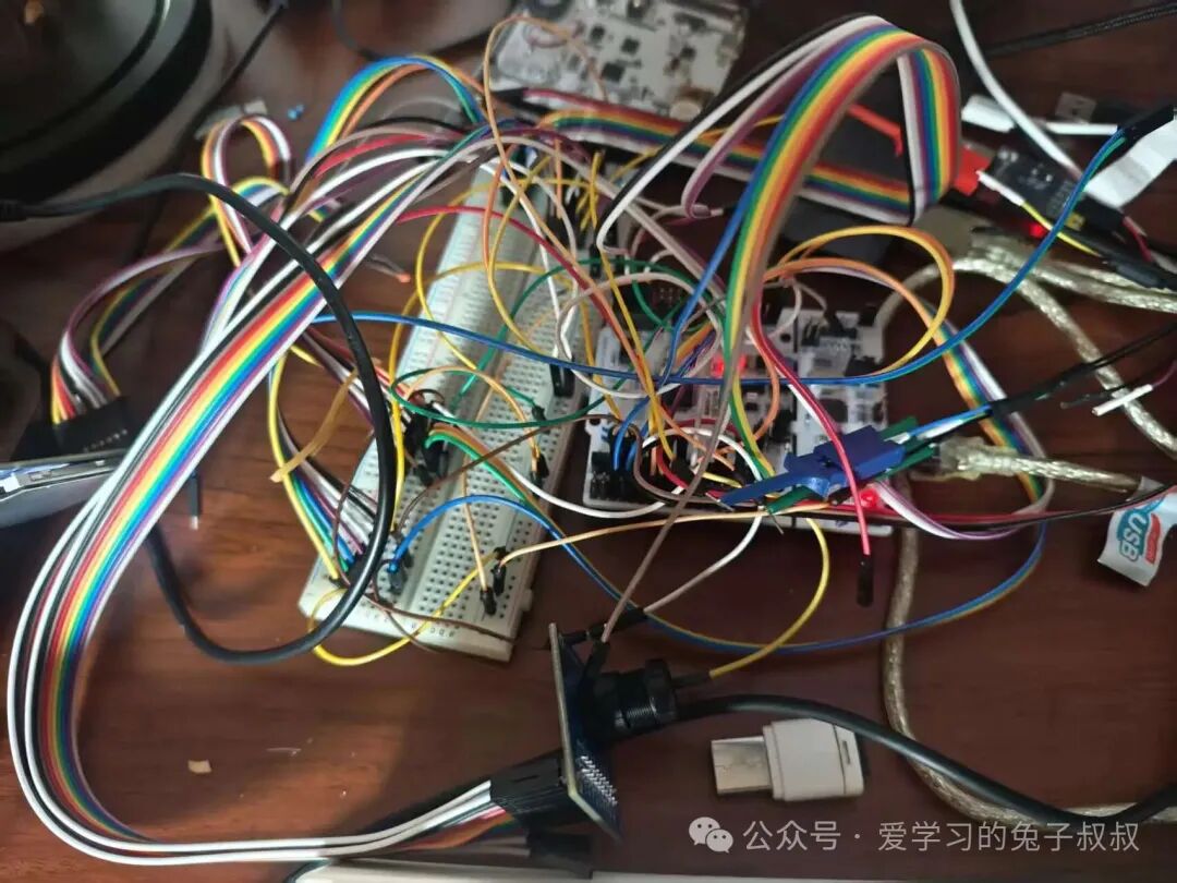
The LCD screen has 16 wires, and the camera has 18 wires, connected through a breadboard. After connecting, it was a bit messy. I also dug a pit for later; the image was always incorrect during display, and I eventually found that the D7 line was not connected~~ It took quite a bit of time to check.
 Software PartThe software part mainly consists of two blocks: one is the SCCB protocol for reading and writing registers, and the other is the timing for reading camera data.SCCB ProtocolSince we use the STM32’s I2C to implement the SCCB protocol, this part is relatively simple.Writing to the register involves three stages: the first stage writes the 7-bit device ID (fixed as 0x42 for the OV7670), plus 1 bit for the read/write flag; the second stage transmits the 8-bit register address; the third stage transmits the 8-bit data. The protocol is fully compatible with I2C, so the write method is as follows:
uint8_t OV7670_Write_Reg(uint8_t reg, uint8_t value) { return HAL_I2C_Mem_Write(&OV7670_I2C_HANDLE, 0x42, reg, I2C_MEMADD_SIZE_8BIT, &value, 1, 1000);}Reading from the register involves four stages: the first stage writes the device ID, the second stage writes the register address, the third stage writes the device ID again, and the fourth stage reads the register value. Here we cannot directly use HAL_I2C_Mem_Read to read because this method does not send a STOP signal before sending a START signal between the first two stages and the last two stages; instead, it sends a Repeat Start signal. However, SCCB requires START and STOP to appear in pairs and does not support RS. Therefore, we simulate the first two and last two stages using Transmit and Receive methods.
uint8_t OV7670_Read_Reg(uint8_t reg) { uint8_t value = 0; HAL_StatusTypeDef status = HAL_I2C_Master_Transmit(&OV7670_I2C_HANDLE, 0x42, ®, 1, 1000); if (status == HAL_OK) { HAL_StatusTypeDef status = HAL_I2C_Master_Receive(&OV7670_I2C_HANDLE, 0x42, &value, 1, 1000); // Read successful if (status == HAL_OK) { return value; } else { return 0xFF; // Indicate error } } else { return 0xFE; // Indicate error }}With the read and write register methods implemented, we can first test whether we can read and write normally by reading registers 0x0A and 0x0B to ensure communication is normal. The values read from these two registers should be 0x76 and 0x73.
uint8_t pid = OV7670_Read_Reg(0x0A); uint8_t ver = OV7670_Read_Reg(0x0B); log_write(LOG_LEVEL_INFO, "OV7670 Register PID:Ver Value: 0x%02X:0x%02X", pid, ver);Register InitializationAfter implementing the SCCB read and write, we can proceed with the register initialization. The OV7670 has over 100 registers, making initialization very complex. There are many examples online, but since I have not been able to display correctly so far, I am not sure what the correct combination is. To display the test pattern, the following register values can be confirmed to work correctly. Below are the specific values and detailed explanations:
const uint8_t ov7670_qvga_rgb565[][2] = { {0x12, 0x14}, // COM7: QVGA, RGB output, no downsample, according to the manual 0x02 is for test color bars, needs to work with bits 7 of 0x70 and 0x71 {0x40, 0xD0}, // COM15: RGB565 full range output {0x11, 0x03}, // CLKRC: Internal clock division, the division factor is input clock frequency/(last five bits + 1), can be set from 0 to 11111. After testing on F103, setting to 3 is our limit at 8MHz; if set to 2, the GPIO and SPI speeds cannot keep up, resulting in desynchronization. {0x42, 0x08}, // COM17: Display DSP color bars // The highest bits of the following two registers can control the style of the test pattern, working with 0x12. Detailed explanation follows, but the default values are set to horizontal and vertical scaling, which I still do not fully understand. // {0x70, 0x3A|0x80}, //SCALING_XSC // {0x71, 0x35|0x80}, //SCALING_YSC // The following several set brightness, contrast, color matrix, etc., copied from the internet; it seems that setting them makes the colors look better {0x55, 0x10}, {0x56, 0x40}, {0x4f, 0xb3}, {0x50, 0xb3}, {0x51, 0x00}, {0x52, 0x3d}, {0x53, 0xa7}, {0x54, 0xe4}, {0x3d, 0xc0}, // Output window settings, 0x17 plus 0x32's [2:0] sets the starting column (11 bits total), 0x18 plus 0x32's [5:3] sets the ending column // 0x19 plus 0x03's [1:0] (10 bits total) sets the starting row, 0x1A plus 0x03's [3:2] sets the ending column. Here we use QVGA resolution, // RGB565 format, so there are 320 columns and 240 rows, with each column's pixels needing two clock cycles for transmission, so the horizontal width is 640, and the row height is 480. // However, the settings for hstart and hstop are quite strange, with stop being less than start, so it adds back after reaching the endpoint. I am not sure why this is set this way, but since everyone does it this way, I copied it for now. // Later we can experiment with what happens if we set HSTART smaller than HSTOP. {0x32, 0x80}, // HREF {0x17, 0x14}, // HSTART {0x18, 0x02}, // HSTOP {0x19, 0x02}, // VSTART {0x1A, 0x7a}, // VSTOP {0x03, 0x0a}, // VREF}After initializing the registers, the main loop is about controlling the timing, with the code and comments as follows:
while (1){ // Our idea is to render one frame each loop, so first set the LCD window and send the write memory command. // To slightly improve speed, data is sent directly using HAL_SPI_Transmit instead of a wrapper method, which saves the operation of setting CS and data mode each time. // Additionally, a single line buffer is used, collecting 640 bytes of data in one go through SPI transmission. LCD_Set_Window(0, 0, 319, 239); LCD_Send_Cmd(0x2c); LCD_CHIP_SELECT(); LCD_MODE_DATA(); // Wait for VSYNC to go low to high and then back low, indicating the start of a complete frame data. while(VSYNC_IS_LOW()); // 0->1 while(VSYNC_IS_HIGH()); // 1->0 for (uint16_t y = 0; y < 240; y++) { while (HREF_IS_LOW()); // 0-> 1, each line must wait for HREF to go low to high to be valid. uint8_t *p = line_buf; // line_buf is uint8_t line_buf[640] for (uint16_t x = 0; x < 320; x++) { while(PLK_IS_LOW()); //0->1 Wait for the pixel clock to go high on the rising edge. high = GPIOC->IDR & 0xFF; // Read the low 8 bits from PC Pin as the high byte of RGB565. while(PLK_IS_HIGH()); //1->0 Wait for the high level to end. while(PLK_IS_LOW()); // 0->1 Wait for the rising edge. low = GPIOC->IDR & 0xFF; // Read the low 8 bits from PC Pin as the low byte of RGB565. while(PLK_IS_HIGH()); //1->0 *p++ = high; // Store the two bytes in the buffer. *p++ = low; // log_write(LOG_LEVEL_INFO, "0x%02X, 0x%02X", high, low); } HAL_SPI_Transmit(&LCD_SPI_HANDLE, line_buf, 640, 50); // Transmit 640 bytes (one row of 320 pixels) at once. while(HREF_IS_HIGH()); //1->0 Wait for the line synchronization signal to go low. } LCD_CHIP_UNSELECT();}Experimental Results, Issues, and AttemptsUnder the above code, the final result is as follows:From the video, you can also feel the frame rate. Below are some other attempts and less successful results:
- Not setting the DSP color bar for COM17 (0x42) and setting Bit[1] of the COM7 (0x12) register to 1. According to the manual, this should enable the color bar, but in reality, it has no effect. However, setting Bit[7] of 0x70 and 0x71 should yield the following results:
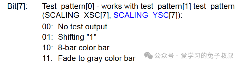 However, these combinations resulted in the following:10: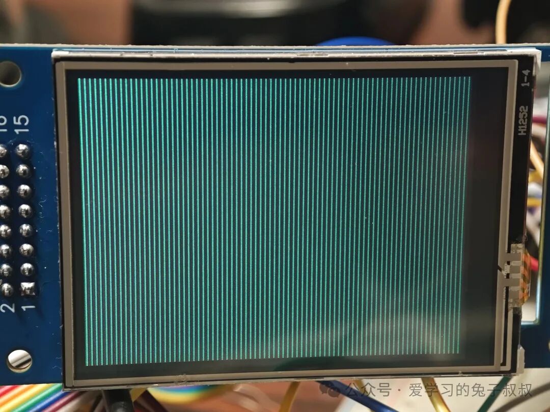
11: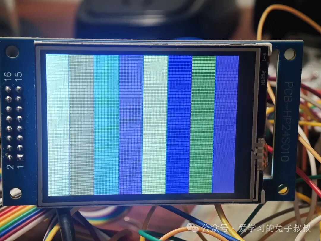 01:
01: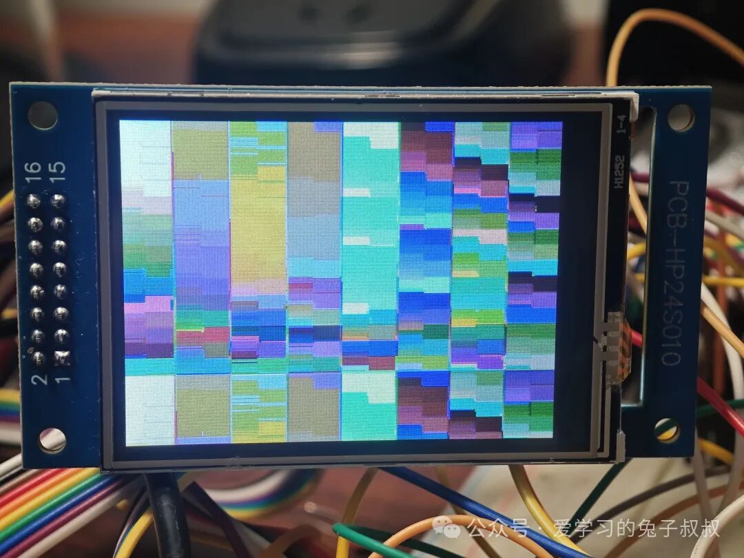 From the results, it appears that the color bar for COM17 (0x42) is independent, while the color bar controlled by Bit[1] of COM7 must work in conjunction with registers 0x70 and 0x71. However, the manual’s description of the combination of Bit[7] of these two registers seems incorrect (reversed? At least 10 is the normal color bar, and it is possible that the manual intended for Bit[7] of 0x71 to be in the high position).
- CLKRC internal clock division, under the current code, can be set to a maximum of 3, which is a division of 4 (input 8MHz, equivalent to an internal clock of 2MHz). If set lower (like 2), it results in desynchronization, leading to results like this:
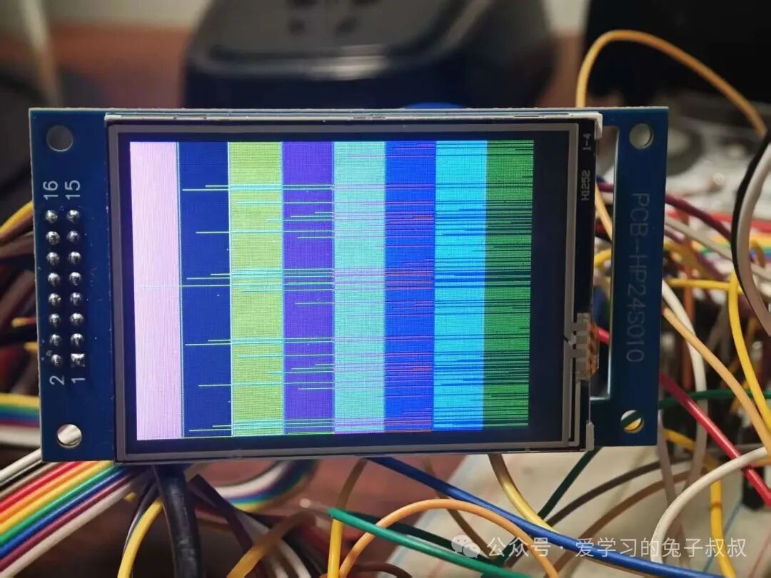
- For non-test images, I do not know the reason, but I have not succeeded; I only see some noise. It is possible that the initialization registers are still incorrectly set, and I have found many similar settings online with similar results. It is also possible that my module has issues? I really have no clue. I hope some experts can provide guidance. The current results, as shown in the video, using various initialization settings from the internet, only differ in pixel color but do not show any fundamental differences.
ConclusionAlthough the final result is still unsuccessful, I have generally understood the underlying working principles and protocols of the camera. Next, I plan to look further into the relevant register initialization parts to see if I can get the image to display.For practical applications, using an STM32F103 microcontroller for video processing is somewhat challenging, with a low frame rate and low practicality. Taking a single photo might still be feasible. It is said that using a camera with FIFO buffer can improve performance; I will try that next time if I have the opportunity.Related code can be found at: https://github.com/sqlxx/stm32-workshop ov7670 branch (Note: The code will continue to change and may not match the description in the text, but it will be guaranteed to run.)