In the field of embedded hardware design, the DDR power circuit serves as the core power supply unit, and its design quality directly affects chip performance and long-term device stability. The RK3588, as a high-performance processor, has stringent requirements for the layout, routing, and component selection of the VCC_DDR power circuit. This article combines official design specifications to dissect the key technical points of DDR power circuit design from five core dimensions: copper coverage, vias, decoupling capacitors, routing topology, and width standards, providing standardized design references for hardware engineers.1. VCC_DDR Copper Coverage: Centered on “Current Demand” to Ensure Smooth Power Supply PathCopper coverage is the “main power artery” of the DDR power circuit, and its design directly determines the efficiency of current transmission and voltage drop control. Two key points must be emphasized:
- Effective Width Calculation PriorityThe copper coverage connected to the RK3588 power pins must meet the maximum current demand of the chip. It is necessary to calculate the effective width in advance using the current-width conversion formula (such as IPC-2221 standard) to avoid local overheating or voltage loss due to insufficient width.
- Avoid Excessive Via SegmentationVias on the copper coverage path can segment the current channel. The number and distribution of vias must be controlled to ensure that each copper path connected to the CPU power PIN is “complete and smooth” without obvious segmentation points.
2. Layer Change Vias and GND Vias: “Quantity Matching” is Key to Decoupling Capacitor EffectivenessWhen the VCC_DDR power requires layer change routing, the via design must follow the principle of “voltage drop reduction, decoupling preservation,” with specific requirements as follows:
- Power Vias: At least 9 in a “Dense Layout”When changing layers, at least 9 power vias with specifications of 0.5*0.3mm must be placed. Increasing the number of vias reduces parasitic inductance and resistance, minimizing voltage drop caused by layer changes and ensuring power integrity.
- GND Vias: “Quantity Equal to” Power ViasThe number of grounding vias for decoupling capacitors must match the corresponding number of power vias. Insufficient GND vias can lead to increased impedance in the capacitor loop, significantly weakening the decoupling capacitor’s ability to suppress power noise, affecting DDR signal stability.
3. Decoupling Capacitor Layout: “Proximity Principle + Precise Alignment” to Maximize Noise Suppression EffectDecoupling capacitors act as the “noise filter” for DDR power, and their layout position directly determines filtering efficiency. The following specifications must be strictly followed (illustrations for clearer understanding):
-
Core Pin Capacitors: Precisely Aligned on the BackAs shown in “Figure 1: Schematic of VCC_DDR Power Pins Decoupling Capacitors for RK3588 Chip,” the decoupling capacitors near the VCC_DDR power pins of the RK3588 must be placed on the PCB back corresponding to the power pins, achieving the shortest path connection between “pin-capacitor” to quickly absorb high-frequency noise near the pins.
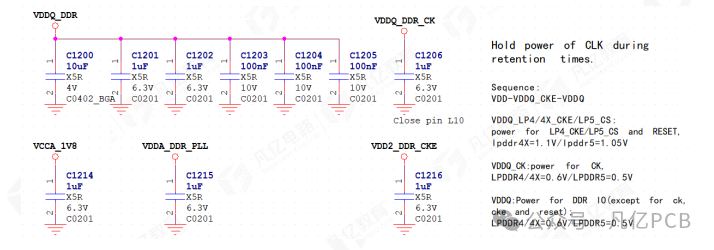 Figure 1: Schematic of VCC_DDR Power Pins Decoupling Capacitors for RK3588 Chip
-
Capacitor GND PAD: “Close to” the Chip Center GND PinThe GND PAD of the decoupling capacitor should be as close as possible to the GND pin at the center of the RK3588 chip to shorten the grounding path, reduce grounding impedance, and prevent noise from coupling to other signals through the grounding loop.
-
Other Capacitors: “Close to Chip” LayoutThe remaining decoupling capacitors for non-core pins should follow the layout logic shown in “Figure 2: Placement of Decoupling Capacitors on the Back of Power Pins,” and be placed as close to the RK3588 chip as possible to ensure all capacitors can effectively suppress noise on the power bus.
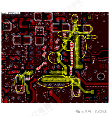 Figure 2: Placement of Decoupling Capacitors on the Back of Power Pins4. Power Pin Routing: “One Via per Pin + Grid Topology” to Optimize Current DistributionThe routing of the VCC_DDR power pins of the RK3588 must adopt a design of “precise matching + topology optimization,” with the following standards:
-
Pins and Vias: One-to-One CorrespondenceEach VCC_DDR power pin must correspond to an independent via to avoid multiple pins sharing a via, which can lead to uneven current distribution and local power supply insufficiency.
-
Top Layer Routing: “Grid” Cross-ConnectionAs shown in “Figure 3: VCC_DDR & VDDQ_DDR Power Pins ‘Grid’ Chain,” the top layer routing must adopt a “grid” topology to achieve uniform current distribution through cross-connections. It is also recommended to control the routing width to 10mil to balance current carrying capacity and routing space requirements.
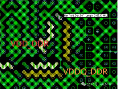 Figure 3: VCC_DDR & VDDQ_DDR Power Pins ‘Grid’ Chain
 -
LPDDR4x Mode: Exclusive Link SchemeWhen the RK3588 is paired with LPDDR4x memory, the layout method must refer to “Figure 4: Power Pin Routing and Vias for RK3588 Chip in LPDDR4x Mode” to adapt to the power supply characteristics of LPDDR4x, ensuring stable high-frequency operation of the memory.
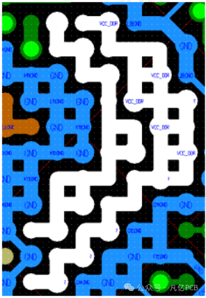 Figure 4: Power Pin Routing and Vias for RK3588 Chip in LPDDR4x Mode5. Width and Copper Coverage: Partition Control, Balancing Current and Space
The width and copper coverage of the VCC_DDR power must be designed according to the “CPU Area” and “Peripheral Area” while coordinating with other signal routing. The specific requirements are as follows:
- Width Hard Standards
- CPU Area (around power pins): Width must not be less than 120mil to meet the current demand for concentrated power supply to the chip pins;
- Peripheral Area (path from power input to CPU): Width must not be less than 200mil to reduce voltage loss during long-distance transmission.
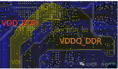
Figure 5: VCC_DDR & VDDQ_DDR Power Layer Copper Coverage for RK3588 Chip
Conclusion: The “Core Logic” of DDR Power Circuit Design
The essence of RK3588 DDR power circuit design is to provide a stable and clean power supply environment for DDR memory through “precise current control, minimized path impedance, and efficient noise suppression.” The five key points mentioned above are interlinked, from copper coverage, vias to capacitor layout, and routing topology, each step must strictly follow the specifications to avoid issues such as device crashes, memory errors, and performance fluctuations due to neglecting details.
For hardware engineers, it is essential to combine the specifications with practical engineering practices, considering factors such as PCB layer count and layout space. Additionally, simulation tools (such as the power integrity analysis feature in Altium Designer) should be used to validate design effectiveness, ensuring the reliability and stability of the final product.
Disclaimer:This article is an original piece by Wanyi Education, please indicate the source when reprinting!For submissions/recruitment/advertising/course cooperation/resource exchange, please add WeChat: 13237418207
“The role of PCB jumpers and correct usage techniques, which 90% of engineers overlook!”
2025-08-30
Newcomers must see! Detailed explanation of Altium PCB spacing rules, making your circuit design more professional and reliable!
2025-08-17
Key points of PCB design: 8-layer/10-layer board recommended stacking + impedance design analysis! (With illustrations)
2025-08-06
2025 New Upgrade | PCB Disciples 2V1, dual mentor project-based teaching takes you directly to engineering positions!
2025-08-04