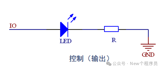
1. What is GPIO?GPIO stands for General Purpose Input Output, which means general input and output ports. For our usage, it is similar to the IO of the 51 microcontroller.Function: It is responsible for collecting information from external devices or controlling the operation of external devices, i.e., input and output.As shown in the figure below, a button controls the change in IO level, and the microcontroller collects the change in IO level.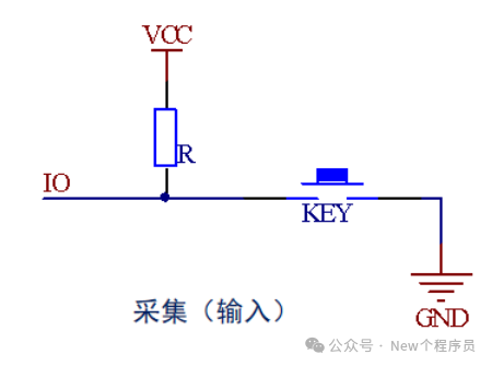 As shown in the figure below, the microcontroller’s IO outputs high and low levels to control the LED light on and off.
 2. GPIO Port Configuration Modes
| Eight GPIO Modes | Characteristics and Applications |
| Input Floating | Used for input, completely floating, presenting a high impedance state, i.e., uncertain state |
| Input Pull-Up | Used for input, internal pull-up, default is high level |
| Input Pull-Down | Used for input, internal pull-down, default is low level |
| Analog Function | ADC, DAC |
| Open-Drain Output | Can only output low level; to output high level, an external pull-up resistor is needed |
| Push-Pull Output | Can output both high and low levels, strong driving capability |
| Open-Drain Multiplexed Function | On-chip peripheral functions (e.g., hardware IIC SDA, SCL pins) |
| Push-Pull Multiplexed Function | On-chip peripheral functions (e.g., hardware SPI SCK, MISO, MOSI pins) |
3. Basic Structure of IO PortsThe basic structure of the IO port is shown in the figure below, referring to STM32F10xxx Technical Reference Manual V10 (Chinese version) Section 8.1. The red box above indicates the route taken by the IO pin for input, while the one below indicates the route for output.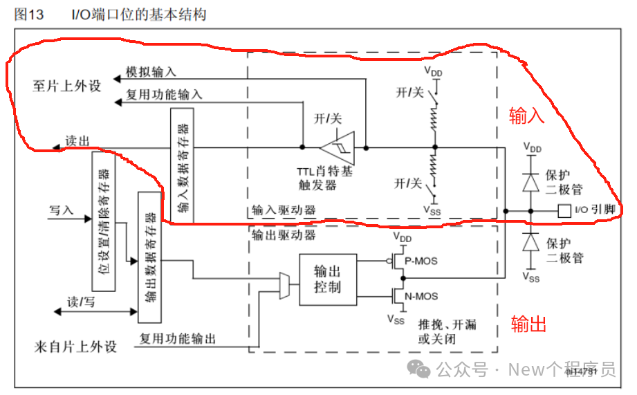 3.1. IO Input
First, starting from the I/O pin, there are two protection diodes, whose main function is to limit the input voltage and protect the internal circuit. The upper diode connects to VDD at 3.3V, and the lower diode connects to VSS at 0V. When the input voltage exceeds 3.3V plus the diode’s forward voltage drop, the upper diode will conduct, and the forward voltage drop of the diode is 0.3V, making the IO pin voltage equal to 3.3V + 0.3V = 3.6V, which does not exceed the VDD voltage required in the datasheet; when the input voltage is less than -0.3V, the lower diode will conduct; if the input voltage is between 0~3.3V, the diodes will not conduct, and normal input will occur.
Next, we come to the pull-up and pull-down resistors. The pull-up resistor connects to VDD, and the pull-down resistor connects to VSS. The on/off state can be configured through the program. If the upper one conducts and the lower one is disconnected, it is pull-up input mode; if the lower one conducts and the upper one is disconnected, it is pull-down input mode; if both are disconnected, it is floating input mode. The purpose of pull-up and pull-down is to provide a default input level. If nothing is connected, the input is in floating mode, and the input level can easily be disturbed. The resistances here are all quite large, representing weak pull-up and weak pull-down, aiming to minimize interference with normal input operations.
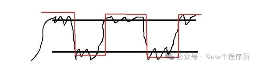
Next, we arrive at the TTL Schmitt Trigger, which is actually a Schmitt trigger; this is a translation error. The function of this Schmitt trigger is to shape the input voltage. Its logic is: if the input voltage exceeds a certain threshold, the output will instantly rise to high level; if the input voltage is below a certain threshold, the output will instantly drop to low level; this effectively avoids input jitter caused by signal fluctuations.
As shown in the figure below, the input voltage is unstable, with two thresholds; above the high threshold or below the high threshold but above the low threshold is considered high level; below the low threshold or above the low threshold but below the high threshold is considered low level.
Next, the on-chip peripherals connect to external devices, including analog inputs connected to the ADC, as the ADC needs to receive analog signals, so it connects to the Schmitt trigger circuit in front. Another is the multiplexed function input, which connects to other peripherals that need to read the port, such as the input pin of the serial port, etc. This line receives digital signals, so it is after the Schmitt trigger.
3.2. IO Output
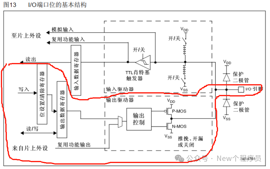
First, the digital part can be controlled by the output data register or on-chip peripherals. If the output data register is chosen for control, it is a normal IO port output; writing a certain bit of this register can operate the corresponding port.
The bit set/clear register can be used to operate a certain bit of the output data register individually without affecting other bits. In C language, this is done using &= and |=; in STM32, the circuit is set up, and only configuration is needed. If we want to set a certain bit to 1 (similar to |=), we write 1 to the corresponding bit of the bit set register, and write 0 to the bits that do not need to be operated; thus, the internal circuit will automatically set the corresponding bit of the output data register to 1, while the bits written as 0 remain unchanged; if we want to set a certain bit to 0 (similar to &=), we write 0 to the corresponding bit of the bit set register, and write 1 to the bits that do not need to be operated.
Next, through output control, we arrive at two MOSFETs, with the upper one being P-MOS and the lower one being N-MOS. This MOSFET acts as an electronic switch, controlled by signals to turn on and off, responsible for connecting the IO port to VDD or VSS. Here, we can choose between push-pull, open-drain, or off output modes.
In push-pull output mode, both P-MOS and N-MOS are active. When the data register is 1, the upper transistor conducts, and the lower one is off, connecting the output directly to VDD, which means outputting high level; when the data register is 0, the lower transistor conducts, and the upper one is off, connecting the output directly to VSS, which means outputting low level; in this mode, both high and low levels have strong driving capability, so push-pull output mode can also be called strong push output mode. In push-pull output mode, STM32 has absolute control over the IO port, and both high and low levels are determined by STM32.
In open-drain output mode, the P-MOS is inactive, and only the N-MOS is working. When the data register is 1, the lower transistor is off, and the output is equivalent to being disconnected, i.e., high impedance mode. When the data register is 0, the lower transistor conducts, and the output connects directly to VSS, which means outputting low level. The function is: it can serve as a driving method for communication protocols. Additionally, open-drain mode can also be used to output 5V level signals, but it must be paired with a pull-up resistor, as it cannot output high level by itself, such as in IIC bus.
4. Conclusion
Finally, this is a brief introduction to STM32 GPIO. If there are any errors, please point them out in the comments, and I will make corrections. Thank you for watching.