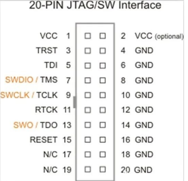
What is a download debugger? In simple terms, a download debugger is a device that converts commands sent from a PC (for example, via USB protocol) into a language that the MCU (which manages the MCU’s internal peripherals) can understand (such as SWD or JTAG protocol), loads code, and precisely controls execution.What is a standard? In simple terms, a standard is a set of rules and protocols that every participant in a specific industry agrees to follow and implement. Microcontrollers that comply with a certain core can use this protocol to download programs.JTAG and SWD are actually both standard protocols. For example, both JTAG and SWD support downloading programs for ARM core microcontrollers.Confusion of debugging protocols Before protocols like SWD and JTAG appeared, debugging and its protocols were chaotic, with each MCU manufacturer proposing their proprietary methods for loading code onto their MCUs. Every time a manufacturer released a new MCU, embedded software engineers needed to understand its proprietary protocol to load code onto the microcontroller.Moreover, debugging adapters were expensive because manufacturers had no competitors that could match their protocols, as the protocols were proprietary. Another reason for their high cost is due to insufficient mass production, as they could only sell debugging adapters to companies (engineers) using the MCUs they manufactured, leading to high production costs.Different protocols can also increase development costs. For example, if you have four different chips from four different manufacturers on your designed board and wish to conduct some automated tests to improve production efficiency, you need to create a super-complex production code that can adapt to this complexity and install four different debuggers at the test points on the board, thereby increasing costs, production time, and programming time.To solve this problem, engineers from major MCU manufacturers and producers have established some standard protocols for debugging, namely the JTAG and SWD protocols described below.1. JTAGJTAG (Joint Test Action Group) is an international standard testing protocol (IEEE 1149.1 compatible), primarily used for internal chip testing. Most advanced devices today support the JTAG protocol, such as DSPs and FPGAs. The JTAG debugging interface must use VCC, GND power signals, and four debugging signals: TMS, TCK, TDI, and TDO, with optional TRST and RESET reset signals and RTCK (synchronous clock) signal. There are two standard connections for JTAG interfaces: 14-pin and 20-pin interfaces.Definitions of 20 PIN JTAG pins:
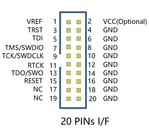
Definitions of 14 PIN JTAG pins:
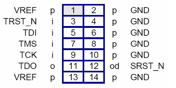
Basic JTAG pins:
VREF: Directly connected to the target board’s VDD, used to detect whether the target board is powered.
TRST: Test Reset, connected to the target CPU’s nTRST, used to reset the CPU debugging interface’s TAP controller.
TDI: Test Data In, connected to the target CPU’s data input signal.
TMS: Test Mode Select, mode selection (control signal) pin.
TCK: Test Clock, clock pin.
TDO: Test Data Out, connected to the target CPU’s data output signal.
2. SWD
SWD: Serial Wire Debug, is a debugging interface protocol designed by ARM for programming and debugging its microcontrollers.
Since SWD specializes in programming and debugging, it has many special features that are usually unavailable elsewhere, such as sending debugging information to a computer via I/O lines. Additionally, because it is specifically made for use in ARM devices, SWD’s performance is typically the best among similar products!
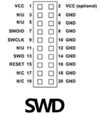
Basic SWD pinsSWDIO: Serial Wire Data Input Output, serial data input/output pin.SWCLK: Serial Wire Clock, serial wire clock pin.SWO: Serial Data Output, the CPU debugging interface can output some debugging information through SWO, this pin is optional.RESET: The system reset signal output from the emulator to the target CPU; it is an optional signal.
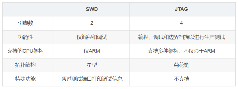
3. Differences Between JTAG and SWD
Advantages of JTAG
1. Not limited to ARM core microcontrollers; it can support debugging and downloading programs for more microcontrollers, such as MSP430.
2. More versatile, used for programming, debugging, and production testing.
Disadvantages of JTAG
It occupies more pins, taking up more board space.
Advantages of SWD
Fewer pins required, only needing SWDIO and SWCLK, which helps save board space.
SWD has special features, such as printing debugging information through its I/O lines.
In high-speed large data situations, SWD’s overall performance is better than JTAG.
Disadvantages of SWD
It can only be used with ARM core microcontrollers.
When to choose SWD over JTAG
-
If your schematic/board design is simple enough to test without JTAG functionality.
-
Debugging performance is more important than production testing, and your device focuses on service research rather than mass production.
-
If the MCU has size limitations, SWD can save space.
-
If your hardware design is too complex, and the MCU has no spare two pins.
4. JLINK
The question at the beginning of the article, what is a download debugger, and JLINK is one type of download debugger.
When the JTAG protocol was defined, computers (PCs) generally had parallel ports, so the connection at the computer end was defined to use parallel ports. However, today, few desktop computers have parallel ports, let alone laptops, and they are increasingly replaced by USB interfaces. So can JTAG support USB protocol and use USB interfaces to debug ARM? This brings us to JLINK and ULINK.
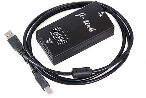
JLINK is a JTAG-based emulator launched by the German company SEGGER. In simple terms, it is a JTAG protocol conversion box, a small USB-to-JTAG conversion box that connects to the computer via USB while still using JTAG protocol to connect to the target board. It completes the conversion from software to hardware.
5. STLINK
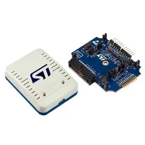
ST-Link is an online debugger and programmer specifically for STM8 and STM32 microcontrollers, also known as a downloader.
ST-Link has communication interfaces such as SWIM, JTAG / SWD for communication with STM8 or STM32 microcontrollers (varies by version).
The official versions of ST-LINK are V1, V2, and V3, with V1 largely replaced by V2. The commonly seen version is V2, while V3 was newly released in the second half of 2018 and is not yet widely available; the commonly seen V2 version is relatively expensive.
Currently, many counterfeit ST-Links on the market are mostly counterfeit V2 standard versions.
The main feature of counterfeit ST-Links is their low price, typically available for 10-20 yuan on online shopping platforms. The internal firmware is generally fine and can be directly upgraded to the official ST firmware, with the main difference being the hardware.
If lucky, it can be used for a long time. Occasionally, there are issues like power short circuits or overheating chips.
Of course, if unlucky, it may break after one download and may even damage your target chip (STM8/32).
6. ULINK
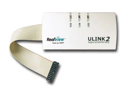
ULINK—ULINK2 is the latest emulator launched by ARM for use with RealView MDK, an upgraded version of the ULink emulator. ULINK2 not only has all the functions of the ULink emulator but also adds support for Serial Wire Debug (SWD), return clock support, and real-time proxy features. Development engineers can easily perform on-chip debugging (using on-chip JTAG, SWD, and OCDS) and Flash programming on target hardware by combining the RealView MDK debugger with ULINK2.
7. Debugger Pin Configuration
There are many MCUs and debugging adapters on the market compatible with SWD and JTAG protocols, which typically implement download and debugging functions through a set of download debugging pins that are internally multiplexed to SWD and JTAG peripherals.
The SWD pins can be multiplexed with JTAG pins under certain conditions, and there are currently many connectors for JTAG and SWD, such as 20-pin connectors:
Of course, there are also 10-pin connectors:
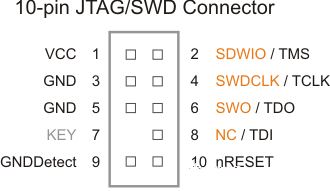
8. Conclusion:
JTAG and SWD are emulator, downloader, and debugger protocol interfaces.
JLink, ULink, and ST-Link are the names of various companies’ emulators, downloaders, and debuggers.
Regularly share embedded knowledge in an easy-to-understand manner,follow our public account, and star it to make progress every day.
Statement:
The copyright of articles and images originally created or reproduced by this account belongs to the original author. If there is any infringement, please contact us for deletion.
Follow, like, watch, and share to support quality content!