ARM’s dominance in the mobile CPU market is well-known, and in the mobile GPU sector, apart from Apple and Qualcomm, most other chip suppliers, such as MTK, Unisoc, and others, predominantly use Mali GPUs. To date, ARM has released five generations of architectures, each serving 3-4 years. These architectures are Utgard, Midgard, Bifrost, Valhall, and Drage. The launch of each generation is closely related to the development of the mobile ecosystem, such as AI, gaming, Android, and the pursuit of optimal PPA (Power, Performance, Area).UtgardThe Mali Utgard GPU is the first generation of Mali GPUs and the first architecture to support OpenGL ES 2.0. This architecture includes the Mali-400, Mali-470, and Mali-450 products, which were available from 2005 to 2015.
The Utgard GPU employs two independent shader core designs:
-
Vertex Shader
-
Fragment Shader
All Utgard GPUs supportsingle vertex shader cores, but the number of shader cores in specific chips may vary. ARM provides configurable design solutions to chip partners, allowing them to flexibly configure GPU specifications based on their performance needs and chip area constraints.
-
Mali-400 and Mali-470 support up to4 fragment shader cores
-
Mali-450 supports up to8 fragment shader cores
The following diagram shows the typical connection of the Mali Utgard GPU to theAdvanced eXtensible Interface (AXI) data bus and the Level 2 Cache (L2 Cache):
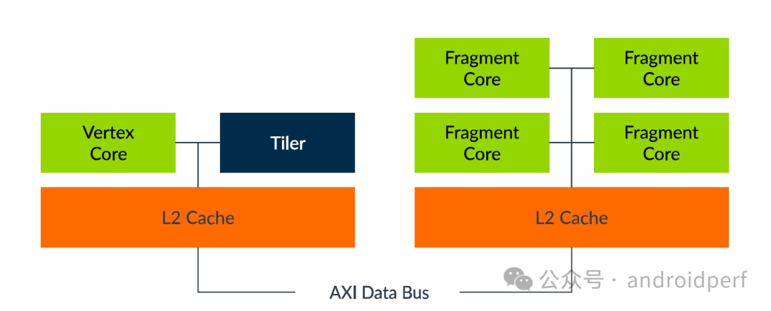
Vertex shader cores and Tiler share a smaller L2 cache, which acts as a buffer for data exchange in the shading pipeline, thereby reducing memory bandwidth usage when the vertex shader passes data to the fixed-function primitive assembly unit.
Fragment shader cores share a larger L2 cache to reduce memory bandwidth consumption due to shared data access (such as vertex inputs or texture data across multiple tiles). The size of this L2 cache is typically32KB per fragment shader core, but ARM’s chip partners can adjust the configuration based on their needs.
The fragment shader cores of the Utgard GPU consist of a programmable pipeline, which is surrounded by fixed-function logic units responsible for:
-
Generating new pixel threads
-
Recycling completed pixel threads
The following diagram illustrates the data flow of the pixel shader core of the Utgard GPU:
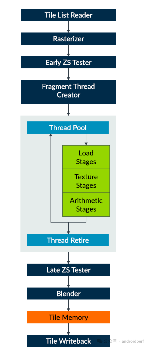
Core Architecture Features
-
Multithreaded Execution Engine
-
Can run128 threads simultaneously, with each thread corresponding to an independent pixel shader program instance
-
High concurrency thread designhides L1 cache misses and memory access latency
Efficient Memory Access Mechanism
-
If data does not hit the L1 cache, it can be fetched directly from the L2 cache with no performance penalty
-
If data needs to be read from main memory, it incurs only a single cycle overhead (depending on memory latency)
Three-Stage Pipeline Design allows the programmable pipeline to enable one of the following processing stages per instruction cycle:
-
Load Stages: Data fetching
The load stage handles all shader memory access operations unrelated to texture sampling, primarily including three types of data access: uniform variable access, varying variable access with interpolation, and thread stack access.
In each clock cycle, the load stage can perform one of the following operations: load 64-bit uniform variable data / interpolate 64-bit varying variable data / load or store 64-bit thread stack data
-
Texture Stages: Texture sampling and filtering
The texture processing stage handles all texture memory access operations, with the following core features:
Basic Texture Throughput Capability
-
Under typical conditions, it can return1 texel processed with bilinear filtering per clock cycle
-
Actual performance varies based on texture format and filtering mode (some special formats may reduce throughput)
YUV Format Direct Read Optimization
-
Supports hardware-level YUV surface direct read (no need to convert to RGB beforehand):
-
When importing YUV data from a camera/video source, each additional plane incurs only 1 clock cycle overhead
-
It is recommended to prioritize the use of semi-planar Y+UV format over fully planar Y+U+V format (as the latter requires more memory accesses)
-
Arithmetic Stages: Mathematical operations
The arithmetic processing unit adopts aSingle Instruction Multiple Data (SIMD) vector processing architecture, with the following core features:
Data parallel processing
-
The Arithmetic Logic Unit (ALU) operates on4-dimensional 16-bit floating-point vectors (vec4 fp16) as the basic operation unit
-
Each pipeline cycle can execute a total of 14 FP16 floating-point operations (FLOPS)
Advantages of SIMD Architecture
-
Basic operations (addition/multiplication)
-
Hardware acceleration support for special functions (such as interpolation, normalization)
-
Single instruction can simultaneously process 4 FP16 components (meeting OpenGL ES/Vulkan floating-point precision requirements)
MidgardARM launched the second generation GPU Midgard in November 2010. The first generation of Midgard products was the first to supportOpenGL ES 3.0 and OpenCL, including Mali-T604/Mali-T658. In August 2012, the second generation of Midgard products was launched, including Mali-T678. In October 2013, the third generation product Mali-T760 was launched; in October 2014, the fourth generation products including Mali-T860, Mali-T830, and Mali-T820 were launched; in February 2015, Mali-T860 was launched. This generation of architecture has a total of 4 generations of products, almost one generation released each year, but the major architecture remains unchanged.In the Midgard architecture, the Tripipe core and unified shader core architecture were introduced.
The Mali Midgard series GPUs adopt a unified shader core architecture, which means that there is only one type of shader processor in its hardware design. This shader processor can execute all types of shader code, including vertex shaders, fragment shaders, and compute shaders. The number of shader cores in specific chips can be flexibly configured, and ARM provides configurable design solutions to chip partners, allowing them to configure the GPU core scale in their specific chipsets based on performance needs and chip area constraints. For example, the Mali-T880 GPU can be configured from a single core (for low-end devices) to 16 cores (for high-performance designs).
To improve performance and reduce memory bandwidth waste caused by redundant data fetching, all shader cores in this architecture share access to the Level 2 cache (L2 Cache). Although the specific capacity of the L2 cache can be configured by chip partners, the typical range is 32-64KB per shader core. Additionally, partners can configure the number of external memory ports and bus width for the L2 cache. The design goal of the Midgard architecture is to achieve a write of 1 32-bit pixel per core per clock cycle, so it can be inferred that an 8-core design should typically have a memory bandwidth of 256 bits (read and write combined) per clock cycle, but this value may vary due to different chipset implementation solutions.
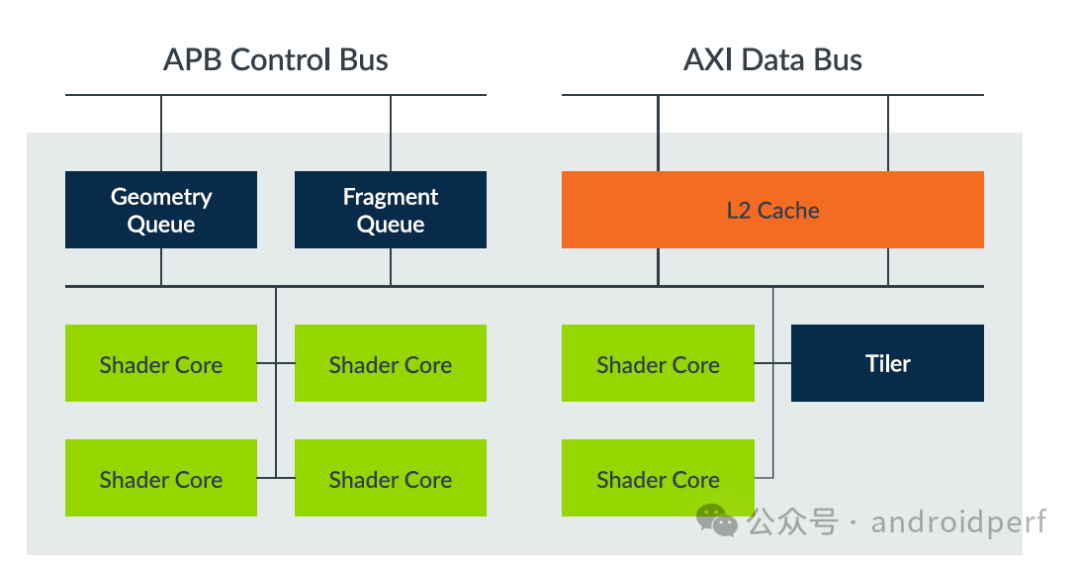
The architecture maximizes hardware resource utilization through a unified shader design, and its flexible configuration scheme can cover various application scenarios from low-power devices to high-performance terminals. The collaborative design of the shared cache mechanism and scalable memory interface effectively optimizes memory bandwidth utilization while ensuring pixel throughput performance. Specific implementation parameters should refer to the final product specifications of each chip manufacturer.
The GPU shader core adopts a collaborative architecture design of programmable Tripipe execution core and fixed-function units. The Tripipe execution core serves as a programmable computing unit, integrating multiple fixed-function modules around it, which are responsible for the preparatory and post-processing work of shader calculations. The following diagram shows the composition structure of the Tripipe execution core and its surrounding fixed-function units:
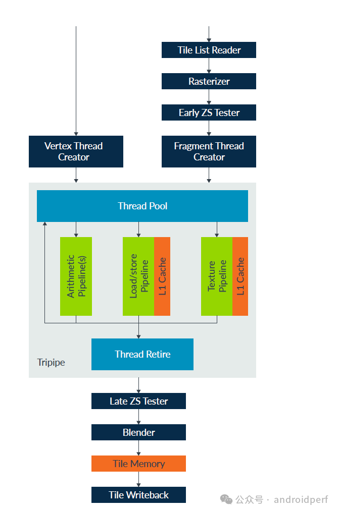
The programmable shader core acts as a multithreaded processing engine, supporting the simultaneous execution of hundreds of threads, with each thread corresponding to an independent shader program instance. By maintaining a large number of active threads, it effectively hides the performance loss caused by cache misses and memory access latency. Even if some threads are stalled due to data fetching, as long as there are ready threads to execute in each clock cycle, performance degradation due to cache misses can be avoided. This architectural design allows for sustained throughput of the computing units even in the presence of memory access latency, and its thread scheduling mechanism ensures maximum utilization of computing resources through hardware-level context switching. The collaborative working mode of fixed-function units and programmable cores guarantees the flexibility of general computing while accelerating key rendering processes through dedicated hardware.
The Tripipe
Tripipe is the programmable part of the shader core responsible for executing shader programs, and it includes the following three types of parallel execution pipelines:• Arithmetic Pipeline (A-pipe): Handles all arithmetic operations• Load/Store Pipeline (LS-pipe): Handles general memory access, varying variable interpolation, and image read/write operations• Texture Pipeline (T-pipe): Handles read-only texture access and texture filtering
All Midgard shader cores include 1 load/store pipeline and 1 texture pipeline, but the number of arithmetic pipelines varies by GPU model:• Mali-T720 and T820 GPUs each include 1 arithmetic pipeline• Mali-T880 includes 3 arithmetic pipelines• The remaining Midgard GPUs are configured with 2 arithmetic pipelines
Bifrost
ARM began launching the Bifrost architecture, the third generation of GPUs, in May 2016, mainly including the Mali-G30, Mali-G50, and Mali-G70 series. The first generation product Mali-G71 was launched in May 2016, the second generation product Mali-G72 was launched in May 2017, and the third generation product Mali-G76 was launched in March 2018.
In the Bifrost architecture, features such as EE core/thread Wrap/Index-Driven Geometry Pipeline were introduced. Performance improved by 40%, and power consumption decreased by 20% compared to Midgard.
The Mali Bifrost series GPUs adopt the same top-level architecture design as the earlier Midgard GPUs, using a unified shader core architecture. This means that the design contains only one type of hardware shader processor, which can execute all types of shader code, including vertex shaders, fragment shaders, and compute kernels.
The number of shader cores in specific chips can be flexibly configured. ARM provides configurable design solutions to chip partners, allowing them to configure the GPU core scale in their specific chipsets based on performance needs and chip area constraints. For example, the Mali-G72 GPU can be configured from a single core (for low-end devices) to 32 cores (for high-performance designs).
To improve performance and reduce memory bandwidth waste caused by redundant data fetching, all shader cores in this architecture share access to the Level 2 cache (L2 Cache). Although the specific capacity of the L2 cache can be configured by chip partners, the typical range is 64-128KB per shader core (specific capacity depends on available chip area). Additionally, partners can configure the number of external memory ports and bus width for the L2 cache.
The design goal of the Bifrost architecture is to achieve a write of 1 32-bit pixel per core per clock cycle, so it can be inferred that an 8-core design should typically have a memory bandwidth of 256 bits (read and write combined) per clock cycle, but this value may vary due to different chipset implementation solutions.
Shader Core
All Mali shader cores adopt an architecture design that surrounds the programmable core with fixed-function hardware modules. The programmable core is the most significant difference between the Bifrost GPU series and the earlier Midgard GPU design. The following diagram shows the implementation scheme of a single execution core and its surrounding fixed-function unit composition:
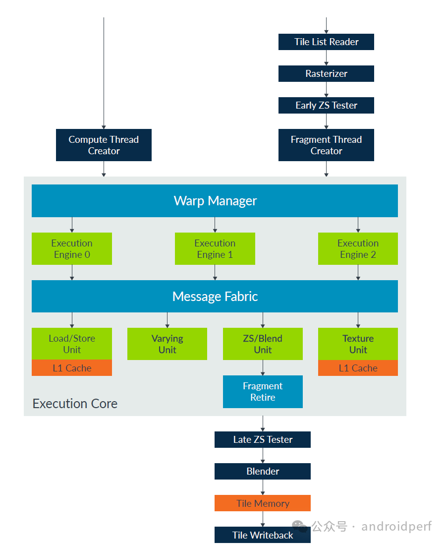
Bifrost GPU’s programmable execution core (EC) consists of one or more execution engines (EE). For example, the Mali-G71 includes three EEs and multiple shared data processing units, which are interconnected through a messaging architecture.
Depending on product configuration, the Bifrost shader core offers two specifications:
-
Small Shader Core: Can read 1 texture sample, blend 1 fragment, and write 1 pixel per clock cycle
-
Large Shader Core: Can read 2 texture samples, blend 2 fragments, and write 2 pixels per clock cycle
The execution engines: Each EE is responsible for executing programmable shader instructions, including: 1 composite arithmetic processing pipeline and the state of the threads processing that instruction.
Thread state: The general register file size implemented for shader programs in the Bifrost GPU is significantly larger than that used in the Mali Midgard GPU. This expanded general register file enhances the performance and scalability of complex programs: programs that maintain full thread occupancy can use up to 32 32-bit registers, while more complex programs can use up to 64 64-bit registers (but at the cost of reduced thread availability). This design allows the compiler to flexibly allocate register resources based on shader complexity through a dynamic balance mechanism between register capacity and thread count—simple shaders can maintain more parallel threads to hide latency, while complex shaders can receive sufficient register support without frequently spilling to memory, thus significantly improving the execution efficiency of complex compute shaders and long pipeline graphics shaders while maintaining the advantages of a unified shader architecture.
Arithmetic processing: To enhance processing speed, a “warp” thread bundle execution mode is adopted:
-
Bundles multiple threads into a warp for parallel processing
-
Optimizes the arithmetic units in the EE based on warp vectorization schemes
Execution characteristics:
-
Single-thread perspective: Presented as a 32-bit scalar operation stream (ensuring effective utilization of hardware by the shader compiler)
-
Underlying hardware: Maintains the efficiency advantage of vector units, with a single set of control logic covering all threads in the entire warp
Load/store unit
The load/store unit is responsible for handling all shader memory access operations unrelated to texture sampling, specifically including: general pointer-based memory access, buffer access, atomic operations, and imageLoad() and imageStore() access for varying image data. This unit can access data in a single 64-byte cache line per clock cycle and reduces unique cache access requests through warp unit access optimization. For example, when all threads access data within the same cache line, the data can be returned in a single cycle. Developers are advised to fully utilize the wide data access and cross-thread merging capabilities of the load/store unit to design shader algorithms, specifically including: using vector load/store operations within threads and allowing threads within a warp to access contiguous address ranges. It should be noted that each core’s load/store unit is equipped with a 16KB L1 data cache and is supported by a shared L2 cache.
Varying unit
The varying interpolation unit is a dedicated fixed-function varying attribute interpolator. This unit ensures high utilization of functional units through warp vectorization technology, with the following core features:
-
Interpolation Throughput Capability
-
Can complete 32-bit data interpolation for each thread in a warp per clock cycle
-
Example: Medium precision (fp16) four-dimensional vector (vec4) interpolation requires 2 clock cycles
-
Precision Efficiency Comparison
-
Medium precision (fp16) interpolation has a double advantage over high precision (fp32):a) Speed improvement of 100% (time taken for the same data amount is halved)b) Energy efficiency significantly optimized
ZS and Blend Unit
The depth stencil (ZS) unit and color blending unit jointly handle all OpenGL ES access and programmable access to the tile buffer, supporting the following functional features:• EXT_shader_pixel_local_storage extension• ARM_shader_framebuffer_fetch extension• ARM_shader_framebuffer_fetch_depth_stencil extension
Depending on the shader core scale, the blending unit can write 1 or 2 fragments to the tile memory per clock cycle. All Mali GPUs natively support high-speed multi-sampling anti-aliasing (MSAA) technology, specifically manifested as:
-
Full-rate fragment blending (maintaining theoretical peak performance even with 4xMSAA enabled)
-
Native optimized 4xMSAA pixel resolution operations
Texture Unit
The texture unit is responsible for all texture memory access operations, providing 16KB L1 data cache for each texel per clock cycle, supported by a shared L2 cache. The architectural performance of this unit is configurable, with its peak texel throughput per clock cycle matching the pixel output rate of the shader core: depending on product configuration, it can support 1 or 2 bilinear-filtered texture samples per clock cycle. Although specific texture formats and filtering modes may affect actual performance, benchmark performance can generally be maintained at the level of 1-2 bilinear-filtered texels per clock cycle for most texture formats. This design, through the collaboration of dedicated L1 cache (16KB per texel) and shared L2 cache, ensures that chip partners can flexibly configure hardware resources based on target application scenarios (e.g., mobile games require 2 samples/cycle, IoT devices require 1 sample/cycle), where dual-sampling configuration achieves performance doubling through parallel filtering units but incurs approximately 35% additional chip area overhead.
Index-Driven Geometry Pipeline
The Bifrost architecture introduces the Index-Driven Vertex Shading (IDVS) geometry processing pipeline, which significantly optimizes the architecture compared to earlier Mali GPUs that required all vertex shading tasks to be completed before primitive culling (which could lead to computation and bandwidth waste for vertices related to culled triangles). The IDVS technology achieves significant optimization by deferring vertex shading until after the primitive culling stage, allowing vertex processing to be executed only for the final visible primitives. In typical application scenarios, this can reduce redundant vertex computation by 30%-50% and decrease geometric processing bandwidth consumption by 15%-20%, making the Bifrost architecture exhibit significant performance advantages in geometry-intensive workloads (such as complex scene CAD rendering or large-scale vegetation rendering).

Processing pipeline before Bifrost
In contrast, the following diagram shows the workflow of the IDVS pipeline: this pipeline first constructs primitives in primitive order and submits shading tasks in stages (splitting the shader into two parts), first executing the position shading stage to complete clipping and culling operations, and then performing varying shading calculations for all visible vertices that were not culled. This innovative architecture splits the traditional single-stage vertex shading into two sub-stages: position shading (calculating only vertex positions) and varying shading (calculating other vertex attributes), allowing approximately 40%-60% of vertices to be culled early after position shading, thus avoiding subsequent varying shading calculations (in typical scenarios, this can reduce vertex processing power consumption by 35%); at the same time, the primitive-order shading task submission mechanism optimizes cache locality, increasing vertex data reuse rates by 2-3 times, ultimately achieving an overall performance improvement of 25%-40% in geometric processing (specific data depends on the efficiency of scene culling).

Processing pipeline in Bifrost architecture
IDVS pipeline process provides the following key optimizations: first, position shading is submitted only for batches of vertices referenced by the index buffer (each batch must contain at least one referenced vertex), allowing vertex shading to skip over unreferenced spatial gaps in the index buffer; secondly, varying shading effectively reduces redundant computation and bandwidth consumption by submitting shading tasks only for primitives that pass through the clipping and culling stages. Additionally, partial de-interleaving of packed vertex buffers can maximize the advantages of the IDVS geometry process—using two packed buffers is recommended: one for attributes affecting position and another for non-position varying attributes, ensuring that non-position varying attributes of culled vertices do not enter the cache (tests show that this optimization can reduce L1 cache pollution by 15-20%, improving effective data hit rates to over 92%, while also reducing geometric processing bandwidth by another 8-12%).
ValhallARM launched the fourth generation GPU Valhall architecture in 2019. The products areMali-G5x and Mali-G7x series. Compared to Bifrost architecture products, their performance and power consumption have improved by 30%.
In May 2019, the first generation Mali-G77 was launched, followed by the second generation product Mali-G78 in May 2020, the third generation product Mali-G710 in May 2021, and the fourth generation product Immortalis-G715 in January 2022, which added hardware ray tracing. The fifth generation product Immortalis-G720 was launched in May 2023.
The Mali Valhall series GPUs continue the top-level architecture design of the previous Bifrost generation, adopting a unified shader core architecture. This architecture contains only one type of hardware shader processor, which can execute all types of shader code, including vertex shaders, fragment shaders, and compute kernels. The number of shader cores in specific chips can be flexibly configured, and ARM provides customizable design solutions to chip partners, allowing them to configure the GPU specifications in their chipsets based on performance needs and chip area constraints.
The Valhall architecture, while maintaining a unified shader core design, achieves a 2x increase in arithmetic logic unit (ALU) throughput per clock cycle compared to Bifrost through an improved instruction set architecture (ISA) and enhanced thread scheduling mechanism. Its configurable core count feature supports flexible deployment from entry-level single-core configurations to high-end 32-core configurations, with the flagship Mali-G710 configurable to have up to 16 shader cores, each equipped with 64KB L1 cache and shared 1-4MB L2 cache, optimizing bandwidth through a 256-bit memory bus.
Shader Core
All Mali shader cores consist of multiple fixed-function hardware modules surrounding a programmable core. The programmable core is the most variable part of the Valhall GPU series, having undergone significant improvements compared to earlier Bifrost designs. The following diagram shows the implementation of a single execution core and its surrounding fixed-function unit:
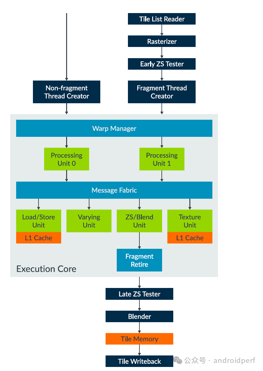
Valhall architecture’s programmable execution core (EC) consists of one or more processing engines (PE). For example, the Mali-G57 and Mali-G77 each include two PEs and multiple shared data processing units, which are interconnected through a messaging architecture. A single Valhall core can achieve: 32 FP32 multiply-add operations (FMA) per clock cycle, read 4 bilinear-filtered texture samples, blend 2 fragments, and write 2 pixels.
The design achieves linear performance scaling through the collaborative work of multiple PEs, with the messaging architecture employing a low-latency ring bus, ensuring that communication delays between PEs are less than 3 clock cycles. Each PE contains independent scalar/vector operation units, supporting mixed precision calculations of FP16/FP32/INT8, while the texture unit adopts a 4-way parallel sampling design, and the blending unit achieves dual pixel output per cycle through dedicated alpha channel acceleration circuits.
Valhall has made the following improvements compared to Bifrost:
Execution Unit Restructuring
-
Adopts ascalar-vector mixed execution model (Bifrost was a pure vector architecture)
-
Arithmetic logic unit (ALU) width reduced from Bifrost’s 16-wide to 8-wide, but achieves double instruction throughput per cycle through dual-issue pipelines
-
Introducesdedicated matrix computation units (supporting FP16/INT8 tensor cores)
Thread Scheduling Optimization
-
Introducesdynamic instruction scheduler (Bifrost used static scheduling)
-
Warp size expanded from Bifrost’s 4 threads to 8 threads
-
Supportsfine-grained thread priority control, enhancing responsiveness for real-time tasks
Memory Subsystem Upgrade
-
L1 cache bandwidth increased by 300% (single core 64KB vs Bifrost’s 16KB)
-
Shared L2 cache supportsnon-uniform memory access protocol (NUMA)
-
Memory compression algorithm efficiency improved by 40% (ASTC/HDR formats)
Geometric Processing Enhancements
-
Second generation IDVS pipeline (Index-Driven Vertex Shading)
-
Position shader throughput increased by 2x
-
Introducesprimitive replay cache (Primitive Replay Cache)
Energy Efficiency Breakthrough
-
Performance/power ratio improved by 50% at the same process node
-
Supportsadaptive clock gating (Per-Core DVFS)
-
Idle power consumption reduced by 30% (through state quick freeze technology)
API Extension Support
-
Natively supports Vulkan 1.2 features (such as Ray Query)
-
Hardware acceleration for variable rate shading (VRS)
-
Enhanced AI inference instruction set (support for INT4/FP8)
DrageCurrently, there is no public information available, but it may include AI-related computations….