Field
Optoelectronic Information
Pain Points
The era of artificial intelligence is driven by massive amounts of data, and data centers, as key infrastructure, are rapidly expanding. To meet the needs for massive data interconnection, optical interconnection technology is widely adopted in data center networks, driving short- and medium-distance optical modules to become a major growth point in the optical communication industry. According to statistics, the top 5 cloud companies globally spent a total of $1.4 billion on data communication optical modules in 2020, and this expenditure is expected to exceed $3 billion by 2026.
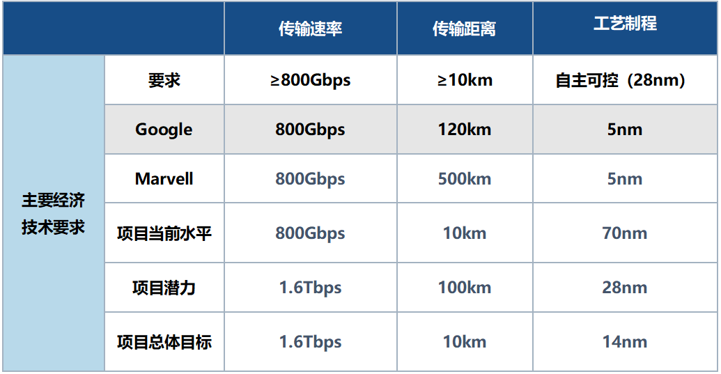
At the same time, with the increase in optical interface rates, the process of DSP chips has evolved from 65nm in 2010 to 7nm in 2022. The next generation of over 800G optical transmission will require the use of 5nm or even 3nm processes to meet requirements, making it difficult to continue relying on DSP electrical domain processing to promote the upgrade of coherent optical module rates.
Additionally, from the perspective of supply chain security, most DSP chips for 400G and over 400G coherent optical modules are monopolized by a few foreign companies. Due to technological blockades, domestic chip processes have been forced back to the 14nm era, posing severe challenges for the autonomy and controllability of high-end coherent optical modules.
Solutions
The essence of the homodyne coherent architecture is to use the originating laser to split and generate a coherent local oscillator at the remote end, which is fed to the receiving end for “homodyne” coherent detection with the modulation signal. The team has conducted sufficient feasibility verification and optimal system design for this architecture in earlier stages. This project further leverages the advantages of coherent optical-electrical fusion signal processing, focusing on two key points: optical-electrical fusion integrated chips and low-power real-time coherent algorithms, aiming to break free from the high dependence of coherent signal processing on advanced processes, manifested as:
(1) “Optical Domain Open Source”: Research on high-speed silicon-based polarization control chips, polarization control algorithms, and their ASIC chips, along with high-speed coherent transceiver chips with polarization control functions. At the system architecture level, by studying adaptive polarization tracking silicon photonic integrated chips that are polarization reciprocal, it compensates for the polarization uncertainty of the local oscillator light and the reverse transmission signal light at a disturbance rate of 600rad/s in an 800Gbps duplex homodyne coherent system, thus exempting from MIMO algorithms, achieving the most simplified coherent DSP architecture to date (“First real-time MIMO-free 800Gb/s DP-64QAM demonstration using bi-directional self-homodyne coherent transceivers” ECOC, 2021, PDP); at the chip level, using optical-electrical fusion research ideas, the highest-speed polarization control chip has been realized, with a tracking speed exceeding 100krad/s (APL Photonics, 9, 066116, 2024).
(2) “Electrical Domain Throttling”: Research on the sources and mechanisms of damage to high baud rate optical signals in homodyne coherent systems, as well as flexible rate digital multi-carrier signal generation technology, to accurately match channel characteristics and enhance system capacity. Meanwhile, developing low-complexity modulation and demodulation algorithms and damage compensation algorithms using Fermat domain signal processing, and studying resolution enhancement, clock synchronization, and new transformation domain equalization technologies for signals under low quantization bit width and low sampling rates, achieving overall optimization of power consumption and performance without loss of performance.
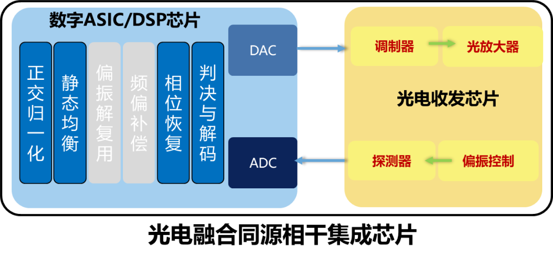
Figure 1 Optical-Electrical Fusion Homodyne Coherent Integrated Chip
Technical Indicators
Competitive Advantages
This project deeply explores the homodyne coherent system and optical-electrical fusion signal processing architecture, proposing a disruptive coherent integrated chip based on optical-electrical fusion, breaking the high dependence of coherent communication on advanced ASIC processes, and overcoming the blockade of high-end DSP chips from foreign countries on China’s optical communication industry, providing a Chinese route for the autonomous controllability and sustainable development of the optical communication industry amidst the wave of de-globalization.
Qualifications and Honors
· The self-homodyne optical communication system has been verified on Alibaba Cloud, and the project “Key Technologies and Industrialization of Open Optical Networks for Cloud Data Center Interconnection” won the second prize of the Science and Technology Award from the China Institute of Communications.
· The optical-electrical fusion homodyne chip won the Excellence Award at the National Disruptive Technology Innovation Competition in 2024.
Technical Maturity
Research and development stage.
Industrial Application
With the rise of AI large models, the computing power demand in data centers doubles every 5 months, leading to exponential expansion in server cluster scale and computing resource allocation. Currently, foreign companies such as Infinera, Cisco, Marvell, and Ciena have developed 800G pluggable coherent optical modules based on 7nm DSP chips, while most DSP chips for 400G and over 400G coherent optical modules are monopolized by a few foreign companies like Marvell (Inphi), Nokia, and Infinera. Due to American technological blockades, domestic chip processes have been forced back to the 14nm era, posing severe challenges for the autonomy and controllability of high-end coherent optical modules. This achievement disruptively proposes a coherent integrated chip based on optical-electrical fusion, breaking the high dependence of coherent communication on advanced ASIC processes and overcoming the blockade of high-end DSP chips from foreign countries on China’s optical communication industry, providing a Chinese route for the autonomous controllability and sustainable development of the optical communication industry amidst the wave of de-globalization.
Application Cases:
The self-homodyne optical communication architecture based on silicon-based polarization control chips has been verified by Huawei, achieving real-time transmission testing at 800Gb/s, becoming a typical architecture for the optical interconnection of next-generation data centers.
Development Plan:
Phase One: Focus on breaking through the key technology challenges of high-speed coherent transmission signal processing surrounding the optical-electrical fusion homodyne chip, developing domestically produced low-cost coherent transmission modules and devices.
Phase Two: Further reduce costs and achieve real-time online transmission at rates not less than 1.6Tbps for 120km.
This project is expected to achieve a prototype system for low-cost coherent optical interconnection in data centers with a single-wave rate of not less than 1.2Tbps for 10km; apply for 20 invention patents; and achieve sales of coherent transmission modules of ≥50 million/year.
Intellectual Property:
This achievement has applied for/authorized multiple Chinese invention patents.
Cooperation Methods:
Patent licensing, patent transfer, equity investment, technology development, negotiation, etc.
Contact Information


Editor | Li Mengnan
Reviewer | Li Zhi