[Topic]: Detailed Analysis of FPGA-Based Sine Wave Generators
[Author]: LinCoding
[Date]: 2016.12.27
[Disclaimer]: Please indicate the source when reprinting or quoting
We all know that FPGA is a digital device, and in the field of communication, it is often necessary to generate a sine wave signal as a modulation signal. The sine wave is generally generated in FPGA using DDS.
DDS (Direct Digital Synthesizer): Direct Digital Frequency Synthesizer.
The main components of DDS include a phase accumulator, phase modulator, waveform data table, DAC, and low-pass filter, as shown in the figure below.
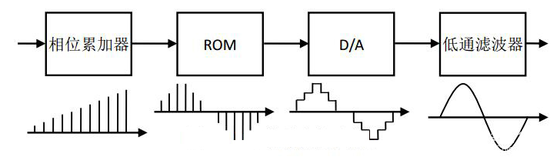
The principle of DDS: First, the sine wave data to be displayed must be stored in ROM. Then, the phase accumulator (which is essentially a counter) continuously accumulates values, using the value of this accumulator as the address for the ROM. The DAC outputs the corresponding voltage value based on the data output from the ROM. However, due to the discreteness of digital signals, the output from the DA will also be discrete voltage values, resulting in a non-smooth sine wave. At this point, simply adding a low-pass filter in the subsequent stage can output a perfect sine wave.
First, let’s look at the figure: Sine Wave
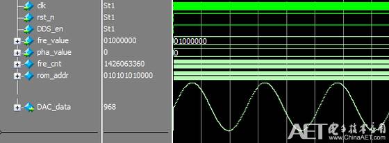
However, the most troublesome aspect of the DDS principle is achieving adjustable frequency: I will explain this in detail below.
First, we need to consider the following two questions:
1. What is the bit width of the phase accumulator (counter)?
2. What are the bit width and depth of the ROM data? (Depth: 2^address bit width)
The first question: The bit width of the phase accumulator is generally between 24 and 32 bits, usually selected as 32 bits. As for why, I am not sure; I couldn’t find an answer online, it may be based on experience. This way, the range of adjustable frequencies can meet most applications.
The second question:
(1) The data bit width of the ROM depends on the DAC module. For example, if the data input range of my DAC module is 0 to 1023, then the data bit width of my ROM should be selected as 10 bits;
(2) The depth of the ROM also depends on your DAC module, as the ROM can only store integers. Even if the adjacent cells in the ROM store values with an interval of 1 (i.e., 1, 2, 3, 4, 5, …), the maximum can only reach 1023, meaning these 1024 data points represent only half a cycle. For a full cycle, it would be 2048 data points, so the standard depth of the ROM is 2^(DAC bit width)*2. However, this is variable; we can store the same number in every two points (e.g., 1, 1, 2, 2, 3, 3, 4, 4, 5, 5, …), making the ROM depth 4096. Of course, I can also store every other point (e.g., 1, 3, 5, 7, 9, …), resulting in a ROM depth of 1024. Therefore, the depth of the ROM is flexible, but the bit width must be determined.
Once these two questions are clarified, the next step is how to achieve adjustable frequency.
Many people indeed find this hard to understand, but it is actually quite simple; it involves playing a digital game, using the low bits to change the speed of high bits. Here’s an example:
//-----------------------------------
//phase adder
reg    [10:0]    fre_cnt;
always @ ( posedge clk or negedge rst_n )
begin
    if ( ! rst_n )
        fre_cnt        <= 11'd0;
    else if ( DDS_en )
        fre_cnt        <= fre_cnt + 1'b1;
    else
        fre_cnt        <= 11'd0;
end
This is the so-called phase accumulator, which counts continuously after DDS_en is enabled until it is full, and then begins counting again. Here, our clk is the system clock at 50Mhz, with a period of 20ns.
DDS_rom u_DDS_ddsrom
(
    .clock            (clk),
    .address          (fre_cnt),
    .q                (DAC_data)
);
Then, we use the counted value as the address for the ROM, and the ROM outputs the corresponding sine wave data. At this point, all 2048 points will be output. Outputting all 2048 points requires 2048*20ns=40960ns, yielding a frequency of 1/(40960ns)=24414.0625Hz, which is the basic frequency of DDS, referred to as the fundamental frequency.
Alright, let’s start changing the frequency.
(1) First, I want to double the frequency. We can do it like this:
//-----------------------------------
//phase adder
reg    [10:0]    fre_cnt;
always @ ( posedge clk or negedge rst_n )       //clk is 50Mhz
begin
    if ( ! rst_n )
        fre_cnt        <= 11'd0;
    else if ( DDS_en )
        fre_cnt        <= fre_cnt + 2'd2;
    else
        fre_cnt        <= 11'd0;
end

DDS_rom u_DDS_ddsrom
(
    .clock            (clk),
    .address          (fre_cnt),
    .q                (DAC_data)
);
In this case, since the clk remains 50Mhz, the counter period is still 20ns. However, we effectively output the ROM data at an interval of 2 points, resulting in only 1024 points being output. Consequently, the output waveform period is 1024*20ns=20480ns, and the frequency is 1/(20480ns)=48848.125Hz, achieving a frequency doubling easily. Of course, I chose integer multiples for clarity; the same principle applies for 1.3x, 1.6x, etc., which is simply changing the counting interval of the counter.
(2) Next, we will reduce the frequency by half. The principle of reducing the frequency is to output the same data every two 20ns (every 40ns). However, we can no longer reduce the counting interval of the counter (it is already at 1), so we must change the clock of the counter. We can do it like this:
//-----------------------------------
//phase adder
reg    [10:0]    fre_cnt;
always @ ( posedge clk_ref or negedge rst_n )    //clk_ref is 25Mhz
begin
    if ( ! rst_n )
        fre_cnt        <= 11'd0;
    else if ( DDS_en )
        fre_cnt        <= fre_cnt + 1'b1;
    else
        fre_cnt        <= 11'd0;
end

DDS_rom u_DDS_ddsrom
(
    .clock            (clk),
    .address          (fre_cnt),
    .q                (DAC_data)
);
The code is the same as the first code, but I used a 25Mhz clk_ref after PLL, resulting in a period of 40ns. In this 40ns, all 2048 points are output, leading to a sine wave period of 2048*40ns=81920ns, and a frequency of 1/(81920ns)=12207.0315Hz, task completed.
However, by doing this, the frequency increase and decrease on the basis of the fundamental frequency are different from the simpler code, and it requires changing the clock of the counter, which we cannot tolerate. Therefore, the improved code is as follows:
//-----------------------------------
//phase adder
reg    [31:0]    fre_cnt;
always @ ( posedge clk or negedge rst_n )    //clk is 50Mhz
begin
    if ( ! rst_n )
        fre_cnt        <= 32'd0;
    else if ( DDS_en )
        fre_cnt        <= fre_cnt + fre_value;
    else
        fre_cnt        <= 32'd0;
end

wire    [11:0]    rom_addr    = fre_cnt[31:20];

DDS_rom u_DDS_ddsrom
(
    .clock            (clk),
    .address          (rom_addr),
    .q                (DAC_data)
);
First, at this point, the clk remains fixed at 50Mhz, and fre_value is referred to as the frequency control word. If fre_value is 1, it means that the ROM address will only increase after counting to 20’h1_00000, which means that every 20’h1_00000*20ns, the output value of the ROM will change. This results in a period of 20’h1_00000*20ns*2048=42.94967296s, and a frequency of 1/43s≈0.023283Hz, which is the minimum frequency achievable by DDS, and all frequencies achievable by DDS are integer multiples of this minimum frequency.
If fre_value equals 20’h1_00000, then every 20ns, the ROM can change its output value, achieving our fundamental frequency, which will not be recalculated here.
So what is the maximum frequency of DDS? We can set fre_value to 32’h8_000_0000, which means the ROM will only output the first value, the middle value, and the last value, resulting in a frequency of 1/40ns=25Mhz. However, the data for these three points in the ROM are all 0, resulting in the waveform being a straight line.
Finally, to improve DDS, we can add a phase adjustment function.
//-----------------------------------
//phase adder
reg    [31:0]    fre_cnt;
always @ ( posedge clk or negedge rst_n )    //clk is 50Mhz
begin
    if ( ! rst_n )
        fre_cnt        <= 32'd0;
    else if ( DDS_en )
        fre_cnt        <= fre_cnt + fre_value;
    else
        fre_cnt        <= 32'd0;
end

wire    [11:0]    rom_addr    = fre_cnt[31:20] + pha_value;;

DDS_rom u_DDS_ddsrom
(
    .clock            (clk),
    .address          (rom_addr),
    .q                (DAC_data)
);
It’s actually quite simple; we just added a pha_value phase control word. Its bit width needs to be the same as that of the DAC module.
Summary:
1. The bit width of the phase accumulator is between 24 and 32 bits, usually selected as 32 bits;
2. The bit width of the frequency control word is the same as that of the phase accumulator;
3. The data bit width of the ROM depends on the DAC module;
4. The depth of the ROM (2^address bit width) has a standard depth but can be arbitrary;
5. The bit width of the phase control word depends on the DAC module.