Translation of Chapter 13 from the compilation “RFSoC-Book” is detailed in the first article of this series.
“An open-source masterpiece, ‘Software Defined Radio Based on Zynq UltraScale+ RFSoC'”
Mr. Big Cat, WeChat public account: Mr. Big Cat’s Little Bookshelf, an open-source masterpiece, ‘Software Defined Radio Based on Zynq UltraScale+ RFSoC’
As a summary of the PL design section, we briefly introduce two types of dedicated hard core modules corresponding to the Gen 1, 2, and 3 RFSoC: RFDC (RF Data Converter) and SD-FEC.
- RF Data Converter IP CoreThe RF Data Converter (RFDC) IP allows the integration of RF-DAC and RF-ADC modules on the chip within the IP Integrator design. Figure 13.6 illustrates the top-level structure of the RFDC IP core, showing the AXI4 interface connecting RFDC with PL/PS, as well as the external interfaces for transmitting and receiving analog signals.
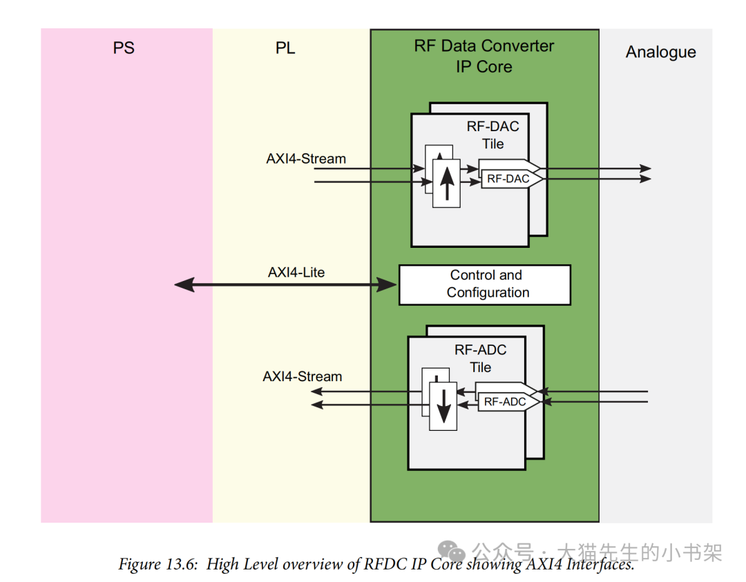
Within this IP core, each RFDC tile is connected to an AXI4-Stream interface, where each RF-ADC tile connects to the master interface, and each RF-DAC tile connects to the slave interface. This allows for the transmission of large amounts of data with RFDC.In the IP Integrator, the RFDC IP core can be configured—either programmatically through Tcl scripts or by setting parameters in the GUI like other standard IPs. Configurable options include enabling or disabling tiles/blocks, setting sampling rates, configuring mixers and decimators, and various operational parameters.The RFDC IP core also includes an AXI4-Lite interface for connecting to the processor in the design (usually the PS). This interface allows for runtime configuration of the RF Data Converter via software drivers without the need to regenerate the bitstream. For time-sensitive applications, configuring directly on the PL side may be more appropriate, as this method typically has lower latency compared to running software drivers on the PS. Additionally, PYNQ provides comprehensive Python drivers that simplify the invocation and management of RFDC.
-
SD-FEC IP Core
The SD-FEC IP core is structurally similar to the RFDC IP, as both connect the internal hard core resources of the chip to a broader PL/PS design via AXI4 interfaces. Figure 13.7 shows the overall structure of the SD-FEC Core and illustrates its input-output connection relationship with the PL.
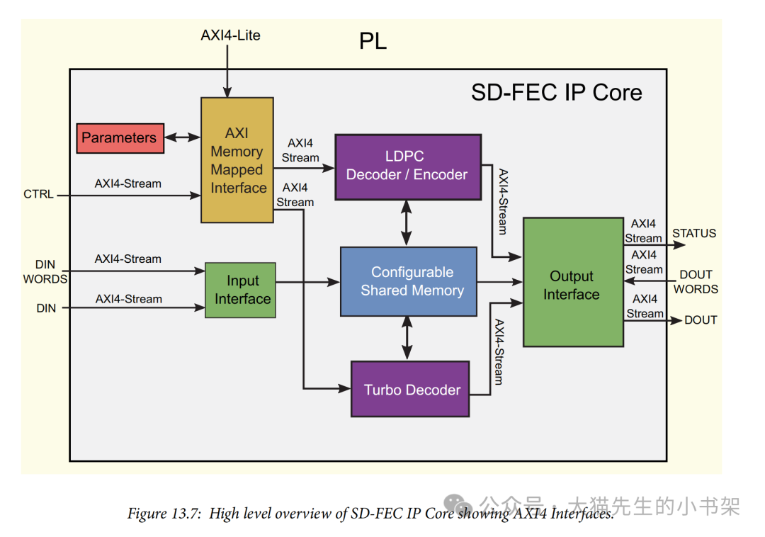
An AXI4-Lite bus connects to the PS to provide parameters such as LDPC coding configuration, which can be controlled via software drivers. Various coding types can be loaded through the AXI-Lite bus; at runtime, a specific coding type can be selected from the loaded coding types via the AXI4-Stream interface (selecting code blocks one by one). The AXI4-Stream interface is also used for input and output data, with parameterizable data dimensions. If design simplification is desired, fixed sizes can be set in the GUI to abstract this part of the detail. The actual design methods for the SD-FEC IP will be discussed in detail in the following chapters.