Mr. Big Cat says:
Translation compilation of Chapter 13 from the book RFSoC-Book, detailed introduction of this book can be found in the first article of this series.
“An open-source masterpiece, ‘Software Defined Radio Based on Zynq UltraScale+ RFSoC'”
Mr. Big Cat, WeChat public account: Mr. Big Cat’s Little Bookcase, an open-source masterpiece, ‘Software Defined Radio Based on Zynq UltraScale+ RFSoC’
Programmable Logic (PL) DesignThe first, second, and third generation devices of the RFSoC family are equipped with a standardized set of FPGA resources, including CLB (Configurable Logic Blocks), DSP48E2 computation units, as well as Block RAM and Ultra RAM storage units. These resources are fully reconfigurable by the user, supporting various application scenarios and usage requirements—PL is particularly suitable for implementing various signal processing algorithms in software-defined radio design.In addition to the logical structure, RFSoC devices also contain various hardened resources, such as SD-FEC modules and RF Data Converters (RFDC). These modules have been detailed in previous chapters. Hardened modules can provide highly optimized implementations for compute-intensive functions, and their operating parameters can be reconfigured based on target applications. For example, in the case of RFDC, adjustable parameters include sampling rate, decimation, and interpolation factors. These resources can be directly connected to the user-configured PL logic structure, enabling the construction of complex designs, such as SDR transceiver systems.When designing RFSoC systems, external interfaces should also be fully considered, especially when using evaluation boards (such as ZCU208 or RFSoC4x2). As mentioned earlier, external RF signals can be transmitted and received via RFDC, baluns, and SMA interfaces. Additionally, external IO can be added as needed, such as external displays, high-speed QSFP data offload interfaces, or Pmod expansion interfaces. These peripheral IOs are realized through reconfigurable connectors within the PL, allowing RFSoC to be integrated as part of a larger system (for example, integrating SDR functions and other subsystems).Next, we will introduce the tools and processes used for developing hardware designs for RFSoC-based SDR systems. We adopt a top-down approach: starting from system-level design and gradually explaining the methods for creating IP modules that constitute the lower levels of the design hierarchy.1. Vivado IP IntegratorVivado IP Integrator (IPI) is the most efficient way to integrate custom hardware logic, pre-built IP cores, and input/output resources. IPI is part of the AMD Vivado Integrated Development Environment (IDE). Users can instantiate and connect pre-generated IP cores in the IPI graphical interface (as shown in Figure 13.2) or programmatically perform the same operations using Tcl (Tool Command Language) scripts.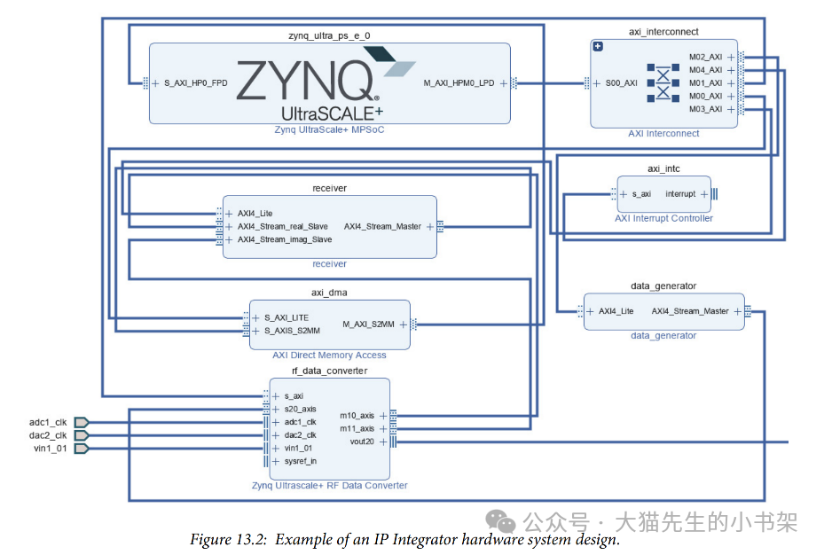 IPI designs are typically formed by connecting multiple IP core instances through interfaces. An interface refers to a set of signals with common functionality. The main advantage of using interface design is the significant reduction in complexity—within the design tool, a graphical connection can represent a group (which can be very large!) of signals and buses. If these signals and buses were to be displayed individually and connected manually one by one, the complexity, workload, and development time of the design would increase significantly. With the interface mechanism, whether a connection is completed once in the IPI graphical interface or through a single Tcl command, the system will automatically establish a complete connection between an IP core and another component in the system.Using interface design also brings the advantage of IPI Design Rule Checks (DRC). These DRCs have a clear understanding of the signals required for different interface types, allowing real-time verification of signal connections. The checking process is performed automatically during design, comparable to the syntax error prompt mechanism in programming languages.When a Vivado project targets a specific evaluation platform (such as the ZCU208 RFSoC development board), the IP Integrator automatically recognizes the available external FPGA pins on that platform. At this point, the IPI’s Connection Automation feature can be utilized to automatically bind the IO ports in the design to the external pins of the development board, significantly reducing manual operations. During this process, the tool automatically generates the corresponding physical pin constraints and clock constraints. Additionally, the IP Integrator will automatically create a top-level wrapper file that defines the interface structure of the entire system in hardware description language (HDL).Example:
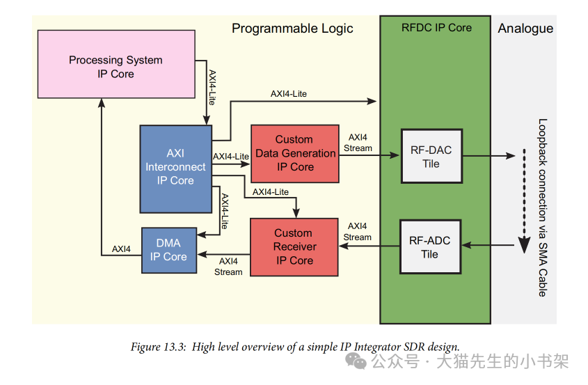 Figure 13.3 shows a conceptual example of an IP Integrator design. This design implements an RFSoC loopback test configuration:The output of the RF-DAC is directly connected back to the RF-ADC input of the same device via SMA cables and an analog filter. In the PL, a custom IP core named “Data Generation” acts as the transmitter, responsible for generating test signals and sending them to the RF-DAC module. After looping back, the signal re-enters the PL through the RF-ADC and is sent to another custom IP core, “Receiver,” which processes the received signal using DSP techniques. Subsequently, a DMA IP core transfers the processed signal to the PS (Processing System) for observation, testing, or demonstration.It is particularly important to highlight a key module in the RFSoC IP Integrator design—the Processing System IP core, which represents the PS part of the device. In this IP core, users can configure various options, including: I/O interface options (such as SPI, I²C); clock options (including peripheral clocks and PL logic clocks); and configurable memory (such as DDR4 memory).2. AXI Interfaces in IP IntegratorOne of the core interface types when using IP Integrator for design is the AXI protocol. AXI is used to connect processing units and IP cores that require high bandwidth and low latency communication. RFSoC implements the fourth generation standard of this protocol—AXI4—in both PL and PS. The AXI4 buses available for RFSoC include three types:
- AXI4: Used for memory-mapped interfaces
- AXI4-Lite: Also used for memory-mapped, but lighter
- AXI4-Stream: Used for point-to-point data stream transmission
IP cores are connected via the AXI4 bus in a Master/Slave manner. Each independent channel within the AXI4 bus contains a set of information signals, as well as tvalid and tready signals, to implement a bidirectional handshake mechanism: the Master side pulls tvalid high to indicate data is available to send, and the Slave side pulls tready high to indicate readiness to receive. When both are valid simultaneously, a valid transfer is completed.In the design shown in Figure 13.3, we can see a typical configuration of the AXI4 protocol, including: AXI4-Stream interfaces between IP cores; AXI4-Lite interfaces between PS and PL (connected via AXI Interconnect IP), and AXI DMA IP core (used for transferring large amounts of data between PL and PS); when designing custom IP cores in external software, ports can be specified as any of the three types of AXI4 buses and can be set as either master or slave interfaces.The three types of AXI4 buses are:
- AXI4 is suitable for scenarios where memory-mapped access is required between processing units (e.g., PS of RFSoC) and IP cores. Its features include: support for single-beat transfers, support for burst transfers of up to 256 beats; support for simultaneous bidirectional data transfers; and five independent channels: read address, read data, write address, write data, and write response. AXI4 is commonly used to transport large blocks of data between main memory and PL IP cores, for example, transferring a large segment of data from PS to PL through multiple bursts of up to 256 elements. In IPI, AXI4 is often used in conjunction with AXI DMA IP Core.
- AXI4-Liteis a streamlined memory-mapped protocol that uses fewer handshake signals, resulting in lower resource overhead compared to AXI4. It also has the same five channels as AXI4, but: only supports single-beat, does not support burst. It is typically used for low bandwidth requirements, such as register configuration of IP cores in PL, driven by access from the PS side.
- AXI4-Streamis used for point-to-point data stream transmission, characterized by: support for burst transfers of unlimited length, no need for address channels, as its purpose is to allow data to flow continuously between IP cores. AXI4-Stream is particularly suitable for real-time signal processing, including: video processing, communication systems, and network data streams. In RFSoC, data between RFDC and PL is transmitted via AXI4-Stream.
3. IP RepositoryVivado supports the use of IP cores to assist in the development of hardware designs. IP cores are essentially independent hardware modules, equivalent to HDL descriptions that can be directly integrated into system designs. Most IP cores are highly parameterizable and stored in an IP repository, allowing designers to reuse them as needed across different projects. AMD provides official IP cores for RFDC and SD-FEC, along with a wealth of high-value DSP and communication IPs that can accelerate SDR hardware design. Additionally, there are many more IP resources available for various applications. These ready-to-use, validated radio-related IP modules are a significant advantage of the RFSoC design ecosystem, significantly shortening the development cycle of SDR systems.In addition to the aforementioned domain-specific IPs, a broader IP catalog also provides general modules, such as DMA (Direct Memory Access) and various peripheral interfaces. Reusing these mature modules can avoid redundant development and testing, allowing designers to focus more on the specific application itself, thereby significantly reducing development workload.For example, Figure 13.4 shows an AXI Interconnect IP core in the Vivado GUI. In IPI, the graphical representation of this IP core will display its IO interfaces for connecting the entire PL design. This IP core includes two input interfaces S00_AXI, S01_AXI, and one output interface M00_AXI. It also provides independent clock ports, allowing designers to assign different clock domains to each interface as needed.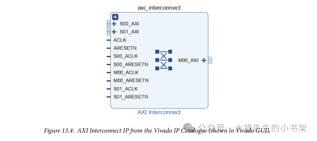 Designers can also develop and encapsulate custom IP cores themselves, even creating their own IP repositories. When a system design requires customized hardware modules, especially those with cross-project reuse value, custom IP becomes particularly important. In the next article, we will introduce various methods for creating custom IP cores.