—–This articleIntroduction—–
Main content includes:
Previous article:I2C Basics (Part 1) — Overview and Data Transmission
This article focuses on: Electrical performance parameters and pull-up resistor calculation
Reference: Official documentation and Chinese translation, reply in the background: I2C
Follow the WeChat public account:Hardware Learning Notes
Reply:Fan Group, to receive materials

—– 正文 —–
First like↓ then read, develop the habit!
1. Electrical Performance
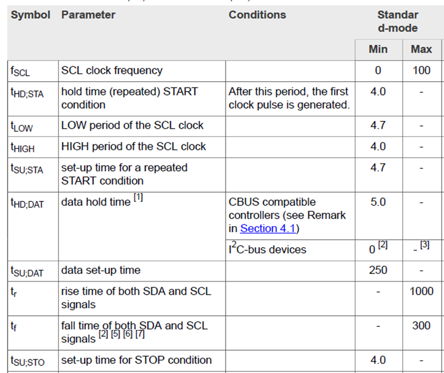
Electrical performance includes the clock frequency,IO levels, timing definitions, etc., which will be introduced one by one below (Note: This article only introduces data in standard mode, for other modes refer to the protocol original document)
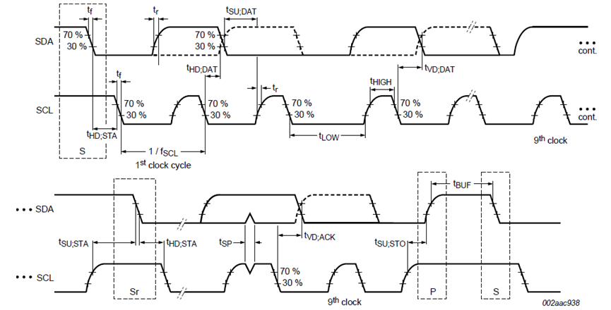
The following timing is common, and the actual I2C waveform in the project must meet these timing requirements, therefore during testing, an oscilloscope should be used to capture the actual waveform and check each timing, of course, the above is just the standard protocol, different device requirements may vary, and the corresponding data sheet should be checked to determine the limits. Other timings can refer to the original text and will not be repeated here.
 1. VIH and VIL
VIH: High-level threshold voltage, only above this voltage is judged as high level, generally taken asVDD+0.5V or5.5V among the smaller values, for example, in a3.3V system, it is taken as3.3+0.5 equals3.8V
VIL: Low-level threshold voltage, only below this voltage is judged as low level, generally the minimum value is-0.5V, the maximum value is0.3VDD, here the maximum and minimum values may vary due to device production errors or slight differences between different devices, the subsequent maximum and minimum values are similar.
 2. tlow
Refers to the low-level duration, which is the timeSDA orSCL is low during one clock cycle below0.3VDD. In standard mode, the minimum is4.7us.
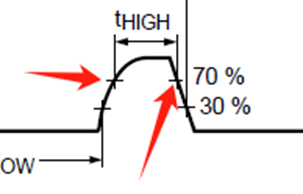
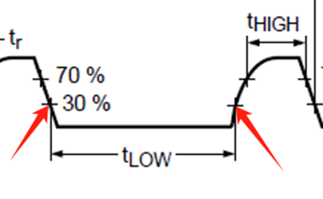 3. tHIGH
Refers to the high-level duration, which is the timeSDA orSCL remains above0.7VDD until the voltage drops below0.7VDD. In standard mode, the minimum is4.0us.
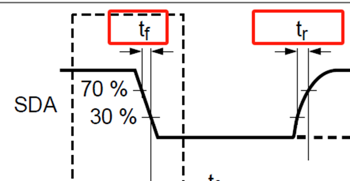
 4. tr and tf
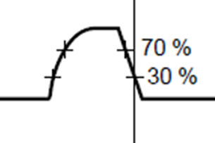
tr refers to the rise time of the data, that is, the timeSDA rises from0.3VDD to0.7VDD, in standard mode, the maximum is1us, minimum is not limited
tf refers to the fall time of the data, that is, the timeSDA falls from0.7VDD to0.3VDD, in standard mode, the maximum is0.3us, minimum is not limited
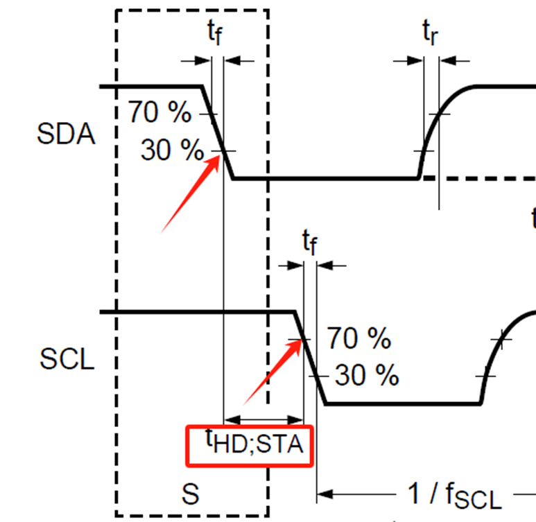
 5. tHD;STA
Refers to the start hold time, when the dataSDA becomes low (SDA below 0.3VDD momentarily starts) untilSCL starts to become low (SCL below 0.7VDD momentarily) this duration, in standard mode, the minimum is4.0us
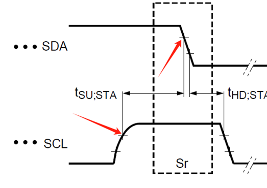
 6. tSU;STA Refers to the start setup time, this timing only occurs after completing the previous data Re-Start, from the moment SCL rises (SCL voltage above 0.7VDD) to the moment SDA starts to go low (SDA below 0.7VDD), in standard mode, the minimum is 4.7us.
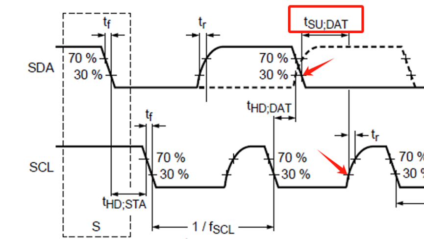
 7. tSU;DAT Refers to the data setup time, the data SDA completes the level change (from SDA 0V to 0.7VDD momentarily or from VDD to 0.3VDD momentarily) until the clock SCL starts to sample (SCL above 0.3VDD), in standard mode, the minimum is 250ns.
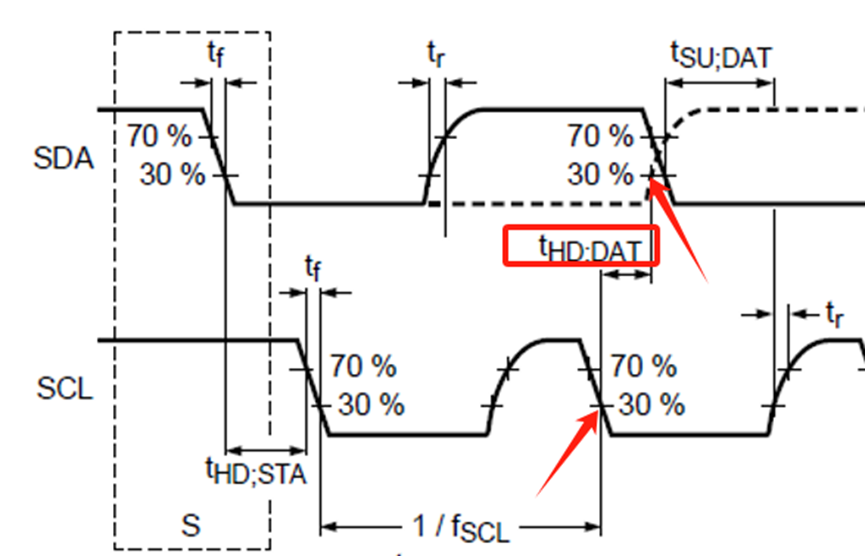
 8. tHD;DAT Refers to the data hold time, from the moment the clock SCL goes low (SCL below 0.3VDD momentarily starts) until the data SDA completes the level change (from SDA 0V to 0.7VDD momentarily or from VDD to 0.3VDD momentarily), in standard mode, the minimum is 5us.
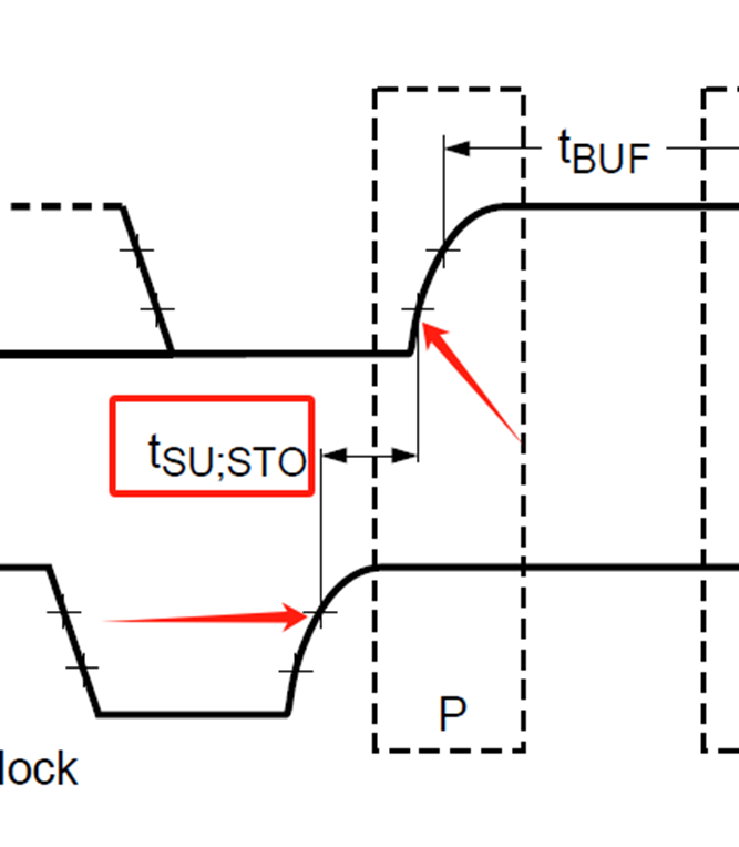
 9. tSU;STO Refers to the stop setup time, from the moment SCL goes high (SCL above 0.7VDD momentarily starts) to the moment SDA starts to go high (SDA above 0.3VDD momentarily) this duration, in standard mode, the minimum is 4.0us.
 2. Pull-up Resistor Calculation For standard mode (i.e., communication speed is 100k), the pull-up resistor is affected by the supply voltage, input current, and bus capacitance, with limited pin input current, generally 3mA, and the maximum bus capacitance Cb is 400pF.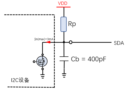
Due to the limited pin input current, excessive values may damage the device, thus the minimum pull-up resistor can be calculated as Rpmin=(VDD-0.3VDD)/0.003, taking 0.3VDD because the maximum low level is 0.3VDD. Calculating with VDD of 3.3V, the minimum value of Rp is (3.3-3.3*0.3)/0.003=0.77kΩ
Additionally, due to the previously mentioned maximum rise time tr (standard mode 1us) affecting the calculation, the maximum pull-up resistor can be calculated.
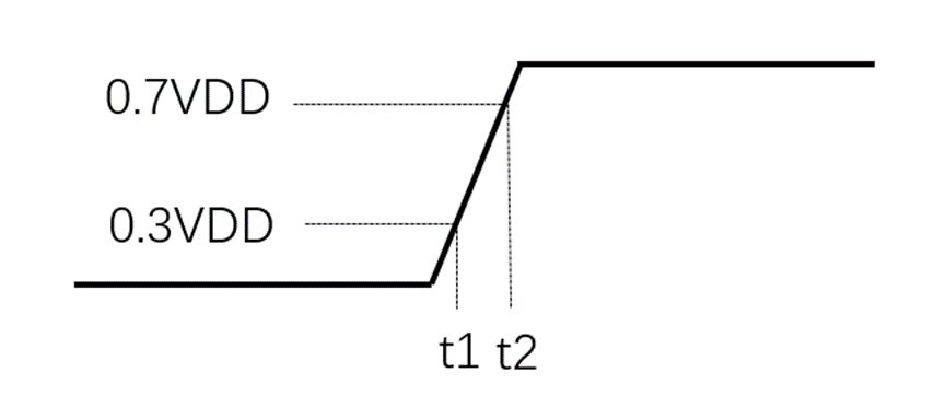
The rise time is actually the process of charging the capacitor Cb, according to the definition of tr, the following equation can be derived: (where R is Rp, C is Cb)
 With tr maximum of 1us, Cb maximum of 400pF calculated: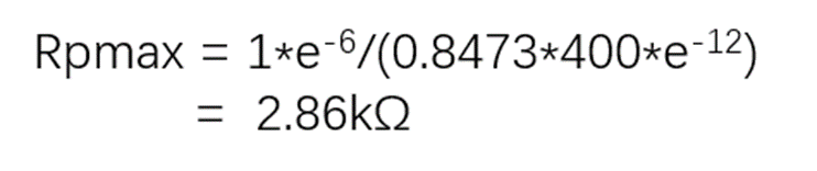
ThereforeRp is in the range of0.77k to2.86k, it is recommended to choose a value close to the middle, and since the actual bus capacitance may not be 400pF, it can also be slightly larger, commonly taken as 4.7k.
Previous article:I2C Basics (Part 1) — Overview and Data Transmission
Welcome to discuss in the comments, don’t forget to like!!!

Click the lower left corner “Read the original text”, materials, books, one-on-one introductory tutoring, all available