In the SMT (Surface Mount Technology) production line, the birth of each circuit board is a game of precision and efficiency. From solder paste printing to component placement, and then to soldering and curing, even the slightest flaw in any link can trigger a “butterfly effect”—leading to unstable product performance at best, or mass rework and even safety incidents at worst. The SPI (Solder Paste Inspection), AOI (Automatic Optical Inspection), and X-Ray are the indispensable “triple guardians” in this game. They build a three-dimensional defense for quality control from different technical perspectives, transitioning electronic manufacturing from “experience-driven” to “data-driven”.
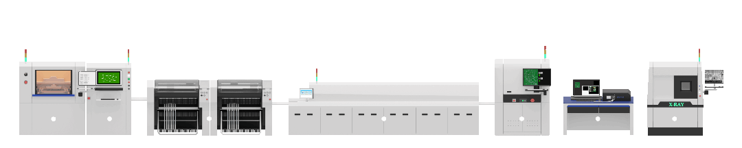
SPI Solder Paste Inspection
SPI (Solder Paste Inspection) is the first quality checkpoint in SMT production, focusing on the precision control of solder paste printing. Its principle is based on optical scanning technology, capturing the three-dimensional shape of solder paste (such as height, volume, area) with high-resolution cameras, and quickly identifying defects such as printing offsets, uneven thickness, and bridging by comparing with preset standards.
In high-speed production lines, the role of SPI is particularly critical. For example, in a circuit board with a 0.4mm pitch BGA package, if the solder paste printing thickness deviates by more than ±10μm, it is easy to encounter cold solder joints or short circuits after reflow soldering. SPI helps engineers adjust printing parameters within seconds through real-time feedback data, reducing the defect rate from 5% to below 0.5%. Additionally, the data statistics function of SPI can provide long-term support for process optimization, such as predicting stencil life by analyzing solder paste collapse trends, thus avoiding mass failures.
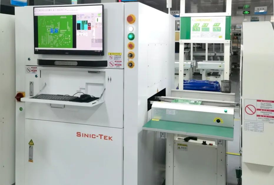
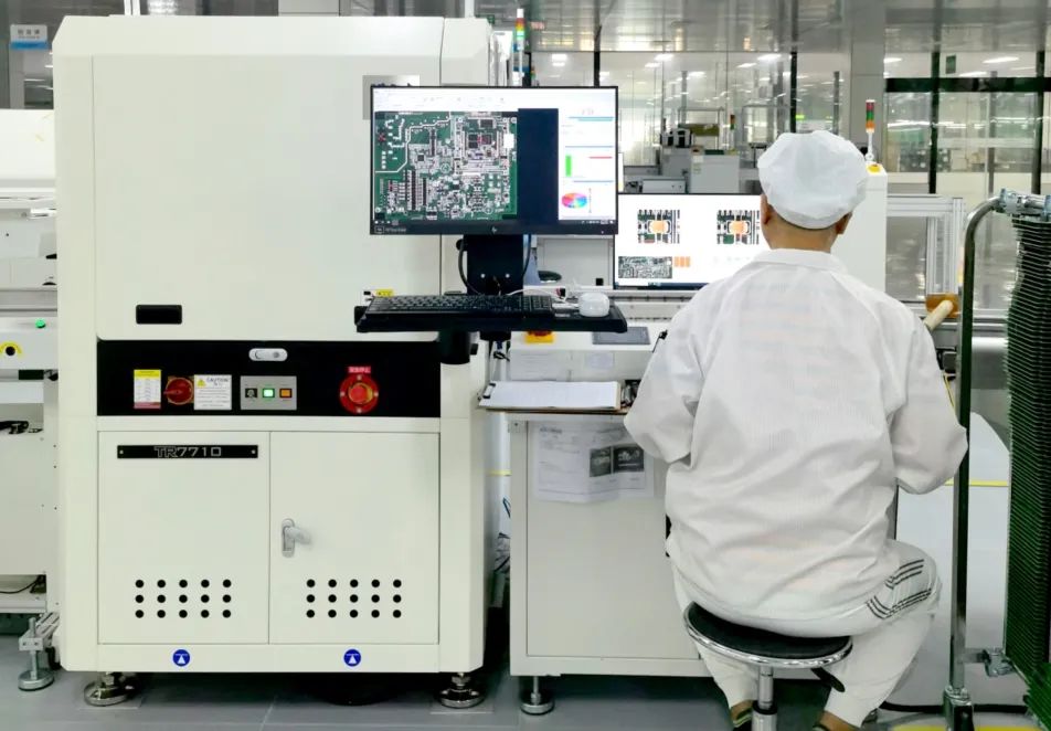
AOI Automatic Optical Inspection
AOI (Automatic Optical Inspection) is the second line of defense in SMT production, responsible for inspecting the quality of component placement and soldering. It scans the circuit board using multi-angle light sources and high-definition CCD cameras to capture appearance information such as component position, polarity, and solder joint shape, and accurately identifies defects such as tombstoning, offset, solder voids, and missing components by comparing with AI algorithms and standard image libraries.
The intelligent characteristics of AOI enable it to adapt to complex scenarios. For example, when inspecting packaged micro-resistors, AOI can identify a placement offset of 0.01mm through sub-pixel level image processing technology; for irregular components (such as connectors and shields), 3D modeling technology is used to ensure a detection coverage rate of over 99.9%. It is worth noting that AOI is typically applied in two stages: pre-reflow AOI focuses on component placement accuracy, while post-reflow AOI emphasizes soldering integrity, with both working together to improve the appearance defect interception rate to over 98%.
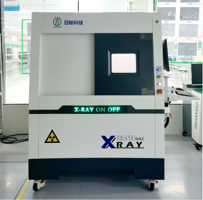
X-Ray Inspection
X-Ray inspection is the ultimate line of defense in SMT production, especially adept at addressing “invisible hazards.” Its principle is based on the penetrating characteristics of X-rays—different densities of materials absorb rays to varying degrees, forming grayscale images that visually display the internal structure of solder joints (such as voids, cracks, bridging) and internal defects of components (such as broken chip leads, encapsulation bubbles).
In high-density packaging (such as 0.3mm pitch BGA) or concealed solder joints (such as QFN bottom pads), the value of X-Ray is irreplaceable. For instance, a medical device manufacturer once faced product failure due to excessive void rates in BGA solder joints. After introducing X-Ray inspection, they adjusted the reflow soldering curve and solder paste formula, reducing the void rate from 15% to below 3%, significantly enhancing product reliability. Furthermore, X-Ray can perform non-destructive testing on PCB inner layer traces and embedded components, providing critical assurance for high-reliability fields (such as aerospace and automotive electronics).
Considerations in Detection Applications
Although SPI, AOI, and X-Ray technologies are already quite mature, maximizing their effectiveness still requires adherence to three key principles:
-
Collaboration rather than isolation: The data linkage between SPI and AOI can predict soldering risks in advance. For example, if SPI detects insufficient solder paste in a certain area, the system can automatically prompt AOI to strengthen solder joint inspection in the corresponding position.
-
Dynamic parameter optimization: The detection accuracy of X-Ray must balance with radiation dosage. For different products (such as flexible circuit boards and rigid boards), parameters like tube voltage and filter must be adjusted to reduce equipment wear while ensuring imaging quality.
-
Talent and algorithms advancing together: The false positive rate of AOI heavily relies on algorithm training. Regularly importing new defect samples and optimizing recognition models with engineers’ experience can reduce the false positive rate from 10% to below 2%.
Yunheng: Comprehensive Inspection Ensuring Product Quality
In Yunheng’s one-stop PCBA service, SPI, AOI, and X-Ray are not only standard in the production process but also the cornerstone of quality commitment.
-
Full process coverage: From solder paste printing to final testing, Yunheng integrates various inspection equipment to ensure 100% detection coverage of critical processes.
-
Data-driven decision making: By real-time aggregating inspection data through the MES system, generating process capability index (CPK) reports, assisting customers in optimizing designs and reducing costs.
-
Customized services: For different fields, Yunheng provides customized inspection processes to ensure products meet design standards.
Conclusion
The collaborative application of SPI, AOI, and X-Ray is not only a stacking of technologies but also a guarantee of product quality. They transform “defect interception” into “defect prevention,” allowing electronic manufacturing to transition from “manpower tactics” to “intelligent closed-loop”. Yunheng, with a complete intelligent manufacturing system, provides reliable full-industry chain services for our smart hardware R&D customers, fully supporting their growth.
◆ ◆ ◆ ◆ ◆