What Is Impedance? Isn’t It The Same As Resistance?
Regarding impedance (Impedance), I have found that many newcomers to this concept often confuse it with resistance (Resistance). This confusion may arise because both terms contain the character for “resistance” in Chinese, and both units are expressed in Ω. Additionally, impedance and resistance are related to the ratio of voltage and current, so it’s understandable that newcomers might think that impedance is just another name for resistance.
“What? The single-ended trace on the PCB must be routed for 50Ω impedance? 50Ω impedance? Are you sure it’s not just a 50Ω resistor?” Newcomers often have such doubts about the routing of transmission lines with specific impedance. Drawing a trace with a resistance value of 50Ω on a PCB seems quite challenging, but in reality, it’s not as difficult as it appears. 
We know that the resistivity of copper is quite low among materials, with graphene at 1.00×10⁻⁸, silver at 1.59×10⁻⁸, copper at 1.7×10⁻⁸, and gold having a higher resistivity than copper, at 2.44×10⁻⁸.
The resistance R of a uniformly dense object with length l (meters) and cross-sectional area A (square meters) can be calculated using R=ρl/A, where ρ is the volume resistivity measured in ohm·meters.
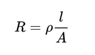
From the formula above, we can intuitively see that the magnitude of resistance is directly proportional to the length l. If the volume resistivity ρ and cross-sectional area A are fixed, then the longer the trace on the PCB, the greater the resistance value. So how long does a trace need to be to achieve a resistance of 50 ohms?
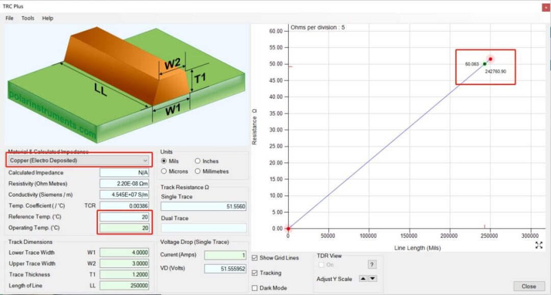
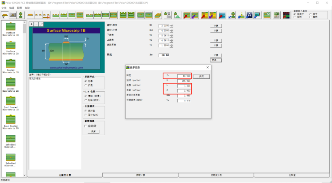
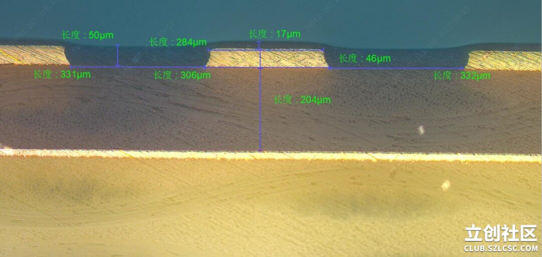
The image above shows the results calculated by the “Line Resistance Calculator” in Si9000, using electrolytic copper foil (ED copper) from rigid copper-clad laminate. T1 represents copper thickness, and W1 and W2 represent trace widths. These three parameters correspond to the cross-sectional area A in the resistance calculation formula; the smaller A is, the greater the resistance. Considering that JLCPCB‘s PCB manufacturing process has a minimum trace width of 3 mils, I chose a trace width of 4 mils here. Due to etching processes, the cross-section of the trace always appears to be a trapezoidal structure, with the etched width of the copper foil adjacent to the substrate always wider than that of the outer copper foil. Here, I am attaching a schematic diagram of the PCB cross-section measurement provided by JLCPCB for better understanding:
The resistivity of copper increases with temperature, so I calculated it at the software’s default value of 20℃.
The calculation results on the right side of the software show the relationship between trace length and trace resistance. According to the parameters calculated above, the trace length needed for a 50Ω resistance is approximately 240,000 mils, which converts to about 6096 mm in metric units. Wow, that’s 6 meters of trace! Is every trace in a DDR layout supposed to be 50Ω? Impossible; there isn’t even enough PCB area to route that! 
Generally speaking, unless for special purposes, we always prefer to keep the routing resistance on the PCB as low as possible. The existence of resistance causes some of the energy guided by the copper traces on the PCB to be converted into Joule heat due to the collisions between free electrons and the lattice, known as ohmic loss, which is responsible for the DC voltage drop (DC IR Drop) and signal amplitude reduction on the PCB.
Impedance Is Not The Same As Resistance
Impedance (Impedance) is a term introduced by British physicist Oliver Heaviside (May 18, 1850 – February 3, 1925). To address the severe signal distortion of transatlantic telegraph cables during long-distance transmission, he began studying the propagation phenomena of electromagnetic waves in transmission lines and derived the telegraph equation (also known as the transmission line equation) based on Kirchhoff’s voltage and current laws, allowing for a simple and intuitive circuit analysis of electromagnetic wave propagation in transmission lines.
A short transmission line or any segment of length ⊿x≤λ/10 can be represented by an equivalent circuit consisting of lumped circuit elements, where λ is the wavelength corresponding to the highest frequency, as shown in the figure below:
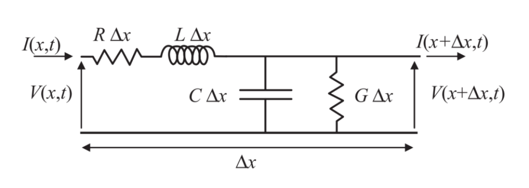
Figure 1: Equivalent circuit of the lumped parameters of the interconnect line’s short section
In the figure, R, L, C, G are the resistance, inductance, capacitance, and conductance parameters per unit length. The premise for obtaining this equivalent circuit is that there are no electric or magnetic field components along the direction of propagation, meaning it is in the transverse electromagnetic (TEM) mode.
For TEM waves, according to the transmission line equation, the characteristic impedance of a lossless transmission line, Z0, is given by:
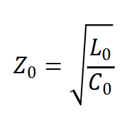
Where L0 and C0 are the distributed inductance and capacitance of the transmission line.
The detailed derivation process can be referenced in the materials provided at the end of this article [1].
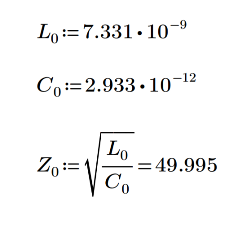
We can verify the relationship between the distributed inductance and capacitance of the transmission line and the characteristic impedance Z0 of a lossless transmission line using the parameters obtained from the lossless calculation mode in the impedance calculation tool Si9000:
Why Control Impedance?
As mentioned in the previous section, Oliver Heaviside proposed the transmission line equation to address the severe signal distortion problem in transatlantic telegraph cables. He introduced the concept of impedance to better guide electromagnetic waves along transmission lines in his published research papers, and he also applied for a patent for the invention of coaxial cables.
Electromagnetic waves possess physical characteristics such as propagation speed, diffraction, interference, refraction, and reflection. When electromagnetic waves propagate along transmission lines, reflections occur at points of impedance discontinuity, which are the primary sources of signal distortion and degradation in signal quality.
The impact of reflections is determined by both the length of the transmission line and the rise/fall time of the signal. A rough rule of thumb is that if the time delay Td generated during signal transmission on the transmission line is less than 20% of the rise/fall time of the signal pulse, then even if reflections occur after the signal reaches the load, the signal at the source end is still in the rising/falling phase, and the reflected signal will be masked by the changing signal.
Another measure to eliminate the impact of signal reflections is to use transmission line structures with impedance matching control. By controlling the geometric structure and layering of traces and reference planes, different forms of transmission lines can be achieved, which requires reasonable arrangement of the layering structure.
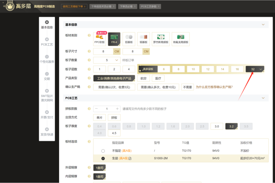
While double-sided boards can also achieve impedance control, achieving 50Ω impedance control requires a significantly larger circuit board area, and as modern electronic products become smaller and more integrated, this brings us to the application of high-layer boards, which can achieve precise layout of functional modules in a very small area while also accommodating countless impedance types.
Producing high-layer boards, compared to single-sided and double-sided boards, involves addressing challenges such as inter-layer connections, inter-layer stacking and alignment, signal integrity, electromagnetic interference, and thermal management, which require very high process capability and precision control. As a professional manufacturer deeply involved in the PCB industry for nearly 20 years, JLCPCB is committed to supporting global hardware innovation and has provided significant assistance in the manufacturing of high-layer boards for electronic product development.
Currently, JLCPCB can manufacture PCBs with up to 32 layers, a minimum hole diameter of 0.15mm, a minimum line width/spacing of 0.0762mm, and supports hundreds of types of lamination structures, sufficient to meet various transmission line structures and multilayer requirements with multiple power/ground planes.

When developing a product, an experienced engineer will consider factors such as manufacturability, cost, and delivery time. Many people have likely encountered situations where designs had to be completely redone, which can be quite frustrating. For impedance, the conventional process involves calculating the impedance value through trace width and spacing, which may require multiple adjustments to achieve the desired impedance. But can you guarantee that the PCB manufacturer can produce this specific trace width and spacing?
To help users avoid unnecessary detours, JLCPCB has created a web tool for complex impedance calculations and provides free lamination structures. What does this look like? Let me continue explaining.
How To Design Impedance That Is Easy For PCB Manufacturers To Control?
From the lossless transmission line calculation formulas above, we know that the characteristic impedance Z0 is influenced by the distributed inductance and capacitance, and theoretically, it can be adjusted by modifying the substrate dielectric thickness, trace width, dielectric constant, and trace thickness on the PCB. However, these parameters are constrained by actual PCB manufacturing, meaning that the designed structure must meet production requirements.
Therefore, designing impedance based on the lamination templates provided by PCB manufacturers is a great starting point.
I remember when I first graduated and started working, I had to contact the PCB manufacturer to obtain impedance templates and negotiate with their sales team. Now, companies like JLCPCB have directly placed impedance templates on their official website:
https://tools.jlc.com/jlcTools/#/impedanceDefaultTemplate
This is indeed much more convenient, and currently, JLCPCB offers over 480 types of impedance templates, covering most common scenarios. Of course, I hope they can also arrange for low-loss board materials in the future. 
Instructions For Using The JLCPCB Impedance Calculation Tool
By comparing the layout of the “Layer Stack” template, you can quickly view the thickness distribution of each layer and the type of glass cloth style used. Personally, I find this selection process quite convenient.
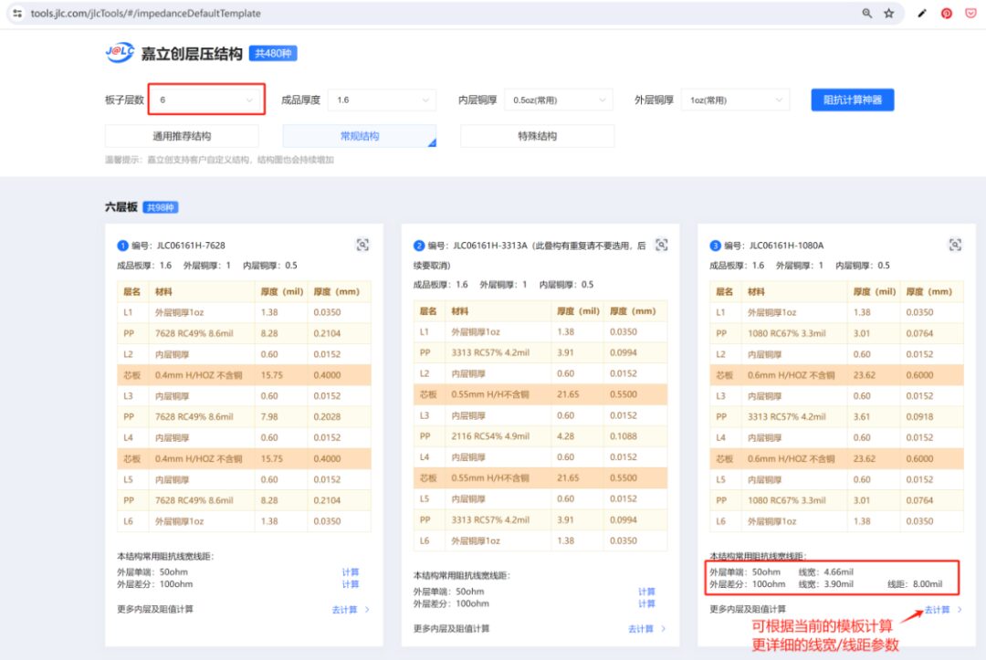
The impedance template provides information on commonly used copper thicknesses, dielectric thicknesses, etc. However, to fill these parameters into Si9000 for verification, we also need the dielectric constant DK information.
JLCPCB will reverse-engineer and fine-tune the actual DK based on the original DK values provided by the substrate manufacturers, combined with the actual measured impedance values. Therefore, the latest dielectric constant values can be found on the JLCPCB website’s “JLCPCB Impedance Calculation Tool Instructions” page, see the link:
https://www.jlc.com/portal/server_guide_37381.html
Impedance Control Verification
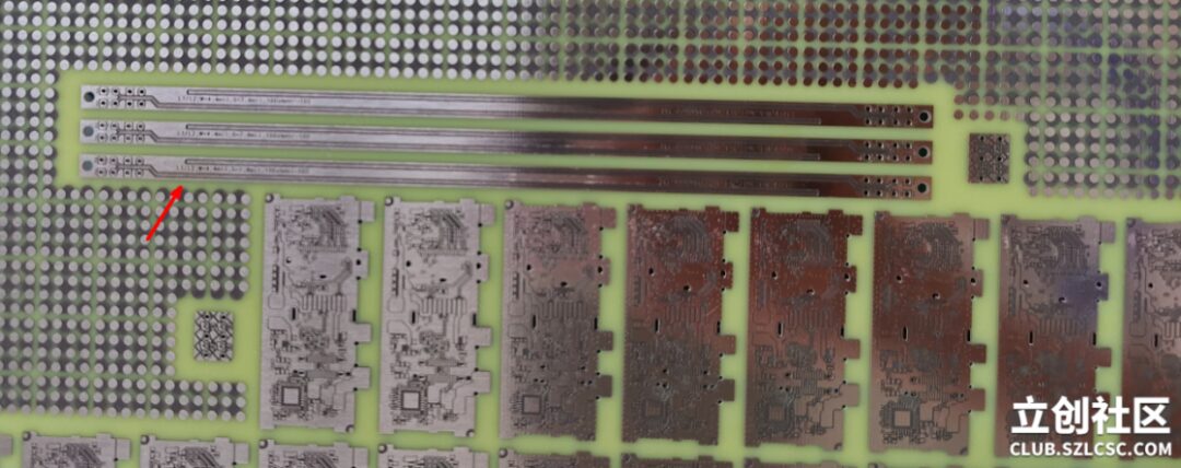
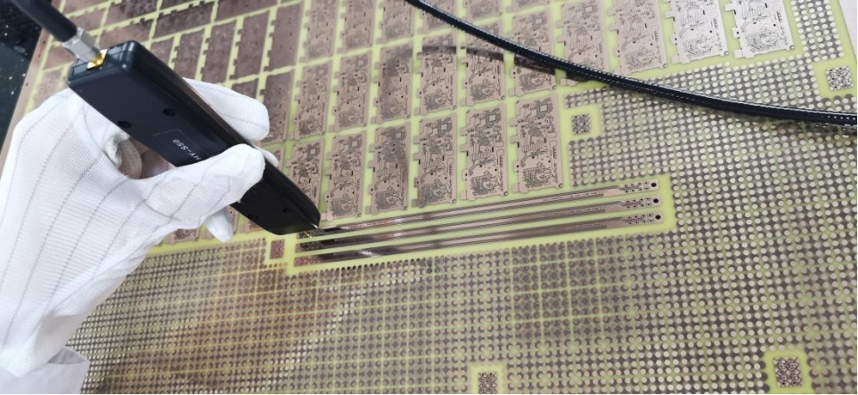
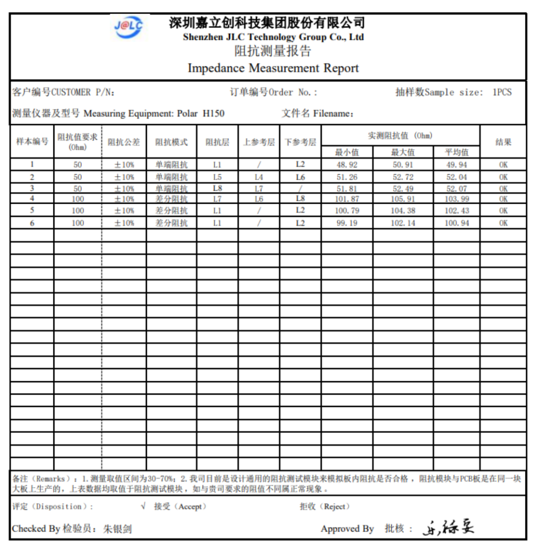
After PCB manufacturing is completed, impedance test strips can be used to verify impedance control (impedance test strips are PCBs used to test the quality of PCB manufacturing processes). Impedance test strips are made on the same panel as the PCB and are usually added at the edges. They are then inspected to ensure layer alignment, proper electrical connections, and cross-sectional checks to examine the internal structure.
Impedance can be tested using Time Domain Reflectometry (TDR). A report will then be generated indicating whether the characteristic impedance has been achieved on the PCB.
Impedance Test Strip
On the JLCPCB ordering page, there is a service for impedance test reports.

Currently, the impedance test report is a paid service. When you place an order and select the need for an impedance test report, JLCPCB will implement special controls during production and will test the impedance upon delivery, which will increase the corresponding cost.

Summary
With the development of high-speed signals, PCB designers need to consider various factors that may affect PCB performance. One of these considerations is impedance control, which is crucial for both signal integrity and electromagnetic compatibility.
JLCPCB provides commonly used lamination templates, with a manufacturing capacity of high-layer boards of up to 32 layers, and offers impedance control during the PCB manufacturing process along with impedance measurement reports, making impedance design on PCBs much simpler.
References
[1]David M. Pozar. Microwave Engineering (Fourth Edition). Tan Yunhua et al. Translated. Beijing: Electronic Industry Press