This article organizes some detailed issues that need attention in layout. Let’s check if you know them all!
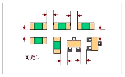
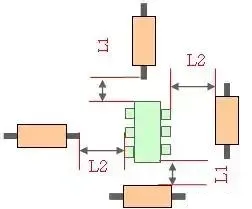
The spacing between surface mount devices is a critical issue that engineers must pay attention to during layout. The spacing between components should not be too large (which wastes PCB space) or too small to avoid solder paste printing adhesion and difficulties in soldering repairs.
-
Same type of components: ≥0.3mm -
Different types of components: ≥0.13*h+0.3mm (h is the maximum height difference of surrounding nearby components) -
For manual soldering and surface mounting, the distance requirement between components: ≥ 1.5mm
*The above suggestions are for reference only and can be designed according to each company’s PCB process specifications.
As shown in the figure above, there should be sufficient distance between through-hole resistors and surface mount devices, recommended to be between 1-3mm. Due to processing difficulties, the use of through-hole components is now rare.
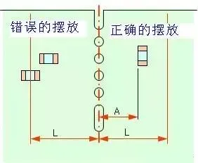
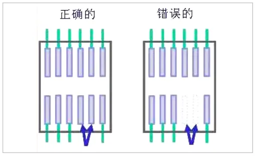
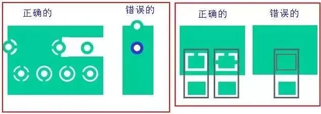
Since PCBs are generally made using panelization, components near the edge need to meet two conditions.
(1) Parallel to the cutting direction. This ensures that the mechanical stress on the components is uniform. For example, if components are arranged as shown on the left in the figure, when the panel is to be split, the stress direction on the two pads may differ, leading to components falling off the pads.
(2) No components should be arranged within a certain distance to prevent damage to components during PCB cutting.

Adding necessary decoupling capacitors on the PCB filters out interference signals from the power supply, stabilizing the power supply signal. It is recommended to connect the power supply to the power pin after filtering through capacitors.
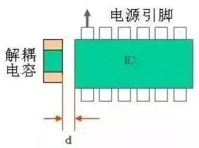
Each IC’s power port needs to have decoupling capacitors placed nearby, as close to the IC’s power port as possible.
When a chip has multiple power ports, decoupling capacitors should be placed for each port.
Crystals, made of quartz, are susceptible to external impacts or falls, so during layout, they should not be placed at the edge of the PCB but as close to the chip as possible.
Crystals should be placed away from heat sources, as high temperatures can also affect the frequency deviation of the crystal.
-
Special high-frequency components should be placed closely together to shorten their connections;
-
Sensitive components should be kept away from noise sources such as clock generators and oscillators;
-
Adjustable inductors, variable capacitors, push-button switches, potentiometers, and other adjustable components should be laid out according to the overall structural requirements for easy adjustment;
-
Heavier components should be fixed with brackets;
-
EMI filters should be placed close to EMI sources.
When designing, PCB engineers must first consider whether the environmental temperature around the electrolytic capacitors meets requirements, and secondly, place the capacitors as far away from heat-generating areas as possible to prevent the internal liquid electrolyte from drying out.
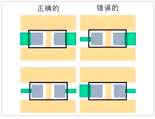
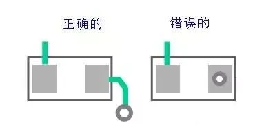
For example, in the case where two pins of a chip are unused, the physical pins still exist. If the pins are left floating as shown on the right in the figure, it can easily cause interference.
If the chip pins are internally unconnected, adding pads and grounding them can avoid interference.
In almost all PCB layouts, vias must be used to provide electrical connections between different layers. PCB design engineers must be particularly careful, as vias introduce inductance and capacitance. In some cases, they can also cause reflections, as the characteristic impedance changes when vias are made in traces.
It is also important to remember that vias increase the length of traces, which need to be matched. If differential traces are used, vias should be avoided as much as possible; if unavoidable, vias should be used on both traces to compensate for the delay in the signal and return path.
Vias should preferably not be placed on pads, as this can easily lead to solder leakage and cold solder joints.
If adjacent pads need to be connected, first confirm the connection outside to prevent bridging, and pay attention to the width of the copper traces at this time.
If pads are in a filled area, the connection of the pads to the fill should be done as shown on the right, and the number of traces connected should be determined based on the current size.
If the left method is used, it will be more difficult to solder or repair components, as the temperature will be dispersed through the copper fill, making it difficult to solder.
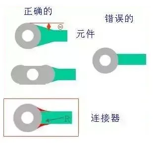
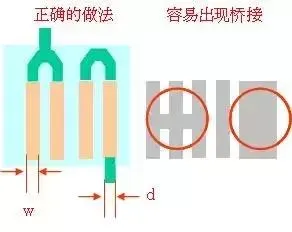
If the trace is smaller than the pad of the through-hole component, a tear drop should be added as shown on the right.
The benefits of adding a tear drop include:
-
Avoid sudden width changes in signal traces that can cause reflections, allowing for a smoother transition between traces and component pads.
-
Solving the problem of connections between pads and traces being prone to breakage due to impact.
-
Setting a tear drop can also make the PCB circuit board look more aesthetically pleasing.
Source: Electronic Product World.
Statement: This article’s copyright belongs to the original author and does not represent the association’s views. The articles promoted by the “Jiangxi Province Electronic Circuit Industry Association” are for sharing purposes only and do not represent this account’s position. For copyright issues, please contact us for deletion.