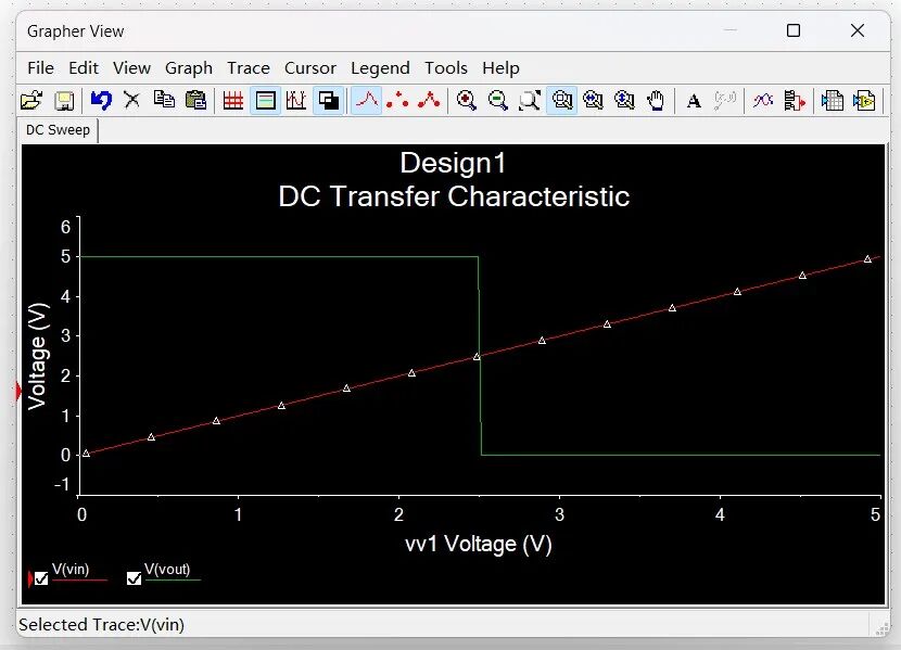
This article demonstrates the construction of a CMOS inverter using P-type Metal-Oxide-Semiconductor (PMOS) and N-type Metal-Oxide-Semiconductor (NMOS) in the NI Multisim simulation software, illustrating the impact of threshold voltage (Vth) on the inverter’s voltage transfer characteristics (VTC).
1. Placing Components
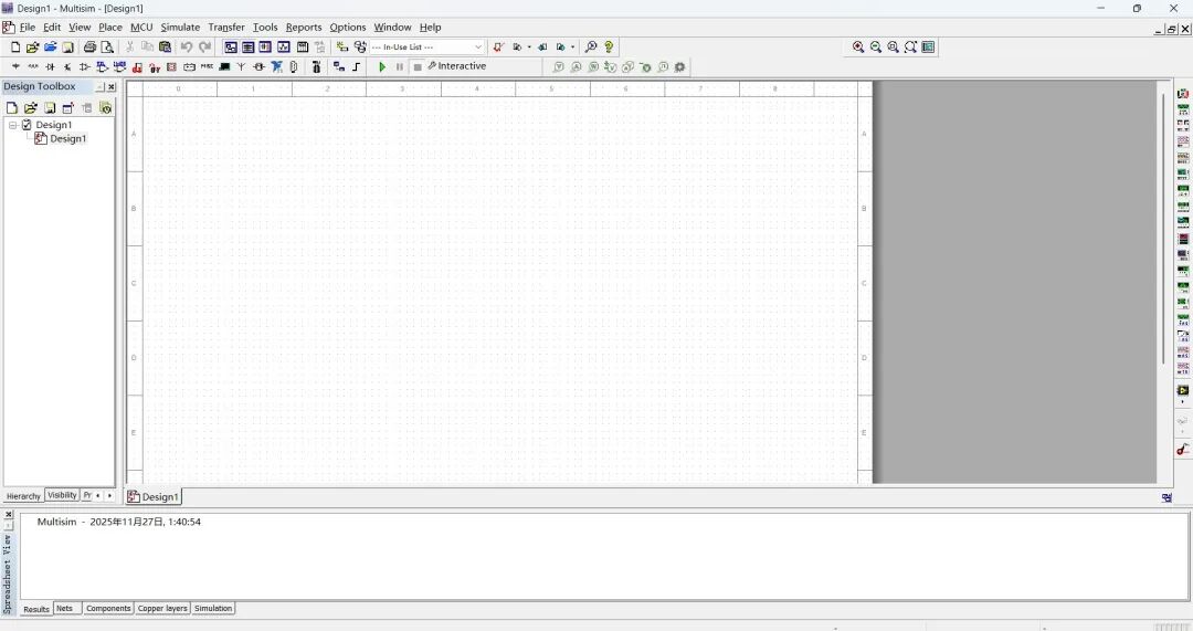
The interface of the Multisim software is shown in the figure below. The top bar is the menu bar, followed by two rows of toolbars. On the left is the design tree, and the large blank area in the middle is where the circuit will be drawn. We will place components here and connect them into a circuit.
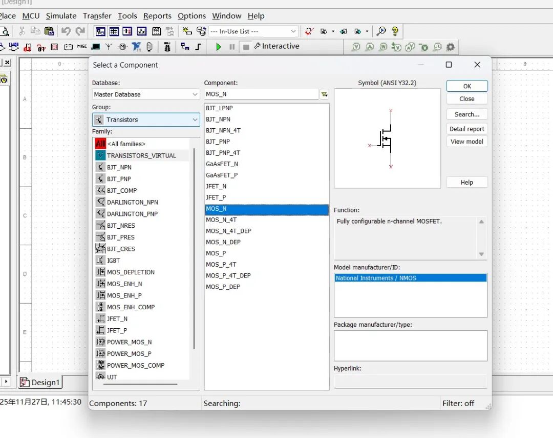
Click on Place->Component to bring up this window, select Transistors in the Group, click on TRANSISTORS_VIRTUAL in the Family, double-click MOS_N to place NMOS, and double-click MOS_P to place PMOS.
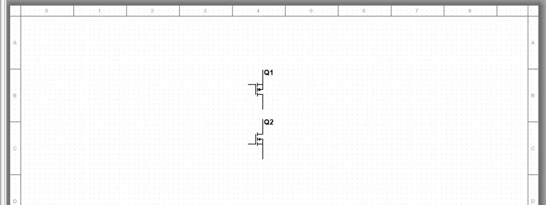
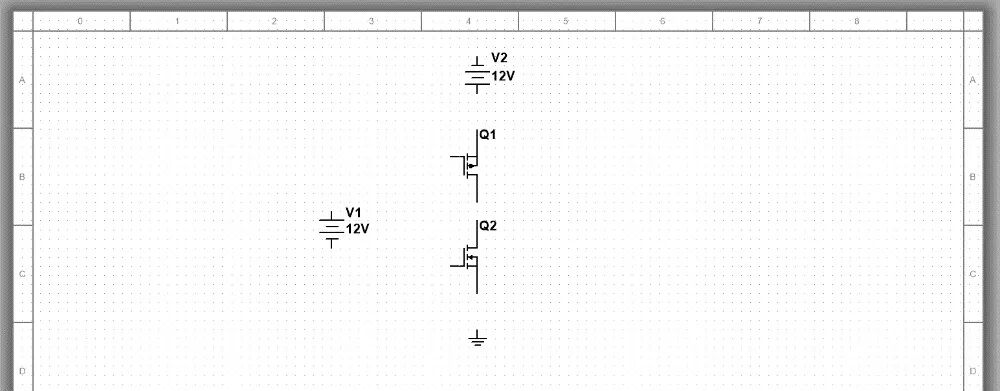
The two types of transistor components are placed as follows: Q1 is PMOS, and Q2 is NMOS. Note their symbol characteristics: the arrow of PMOS points away from the gate, while the arrow in NMOS points towards the gate. If the orientation of the components is incorrect, you can right-click on the component and select flip or rotate.
Place the power supply and ground terminal. In the Group, select Sources, and in the Family, select POWER_SOURCES, placing two DC_POWER supplies and one GROUND terminal.
The following figure shows the situation after all components have been placed. Do not change the parameters of each component yet.
2. Connecting the Circuit
Connect the various parts using wires by clicking on the terminals of the components. After connecting, the gates of PMOS and NMOS are connected to the same power supply, while their source and drain are connected in series to another power supply.
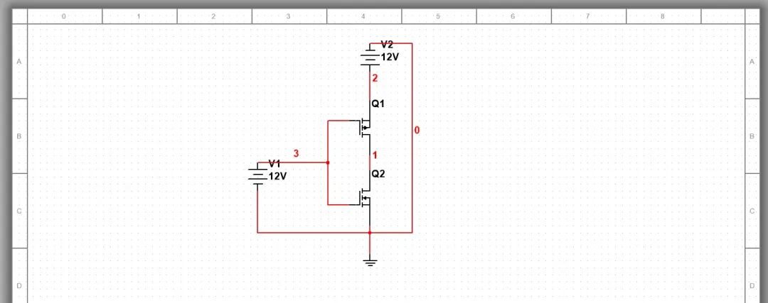
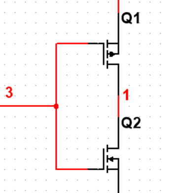
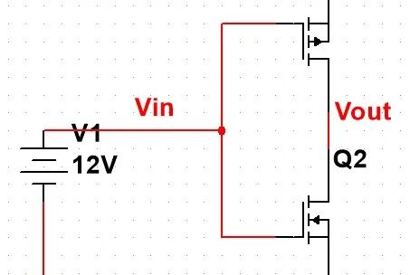
At this point, we have obtained an inverter. The core part of the inverter is the series connection of PMOS and NMOS. The voltage on wire 3 is referred to as the input voltage (Vin), while the voltage on wire 1 is the output voltage (Vout). An ideal inverter has completely opposite input and output: a low input voltage results in a high output voltage, and a high input voltage results in a low output voltage.
Before simulating the inverter characteristics, we can first look at how to modify the component parameters.
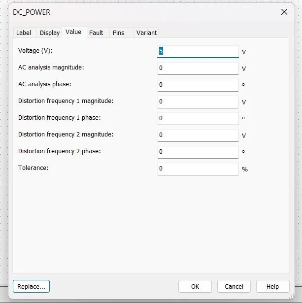
Double-click on V2, and in the pop-up window, change the voltage value of power supply V2 to 5V in the Value tab.
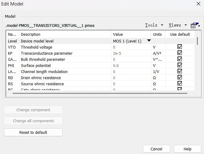
Double-click on the PMOS or NMOS component, click on the edit model in the Value tab, and in the pop-up window, find all the parameters of the transistor. You can see that the default value of the threshold voltage (Threshold voltage) is 0 V.
3. Inverter Simulation
After constructing the circuit and modifying the component parameters, we can start the simulation.
I want to obtain the relationship between the input voltage and output voltage of the inverter, which is the VTC. This can be achieved by applying voltage to V1 and monitoring Vin and Vout. (Note: Right-click on the wire to open the properties window to change the wire name.)
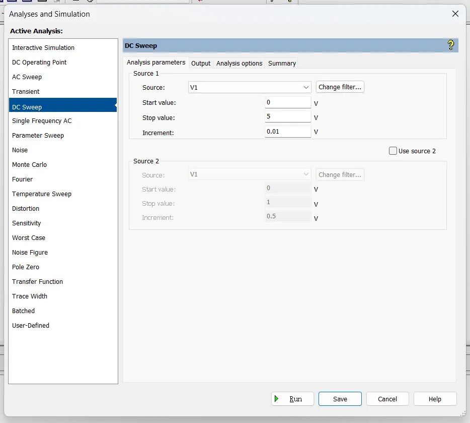
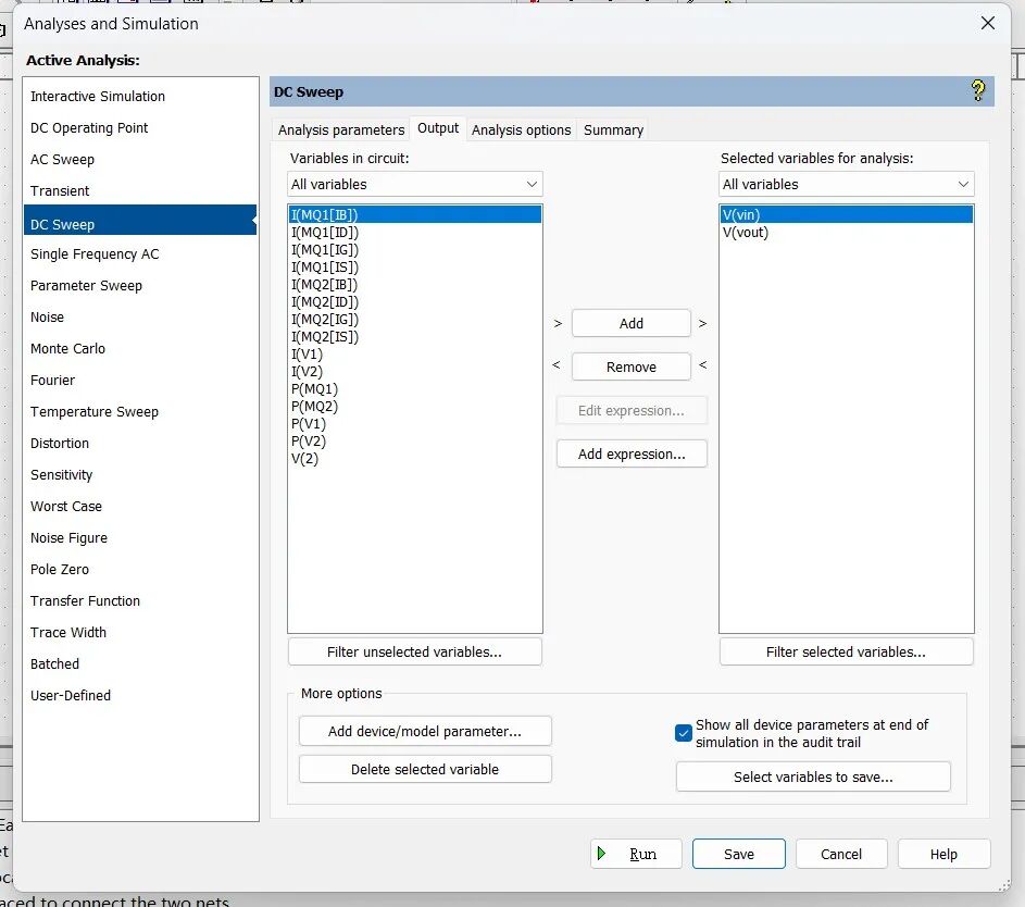
Click on Simulate->Analyses and simulation in the menu bar, select DC Sweep. In the Analysis parameters tab, select V1 as the Source, set the scan range from 0 to 5 V, and the step size to 0.01 V.
In the Output tab, add V(vin) and V(vout) from the left to the right, and then click Run at the bottom to start the simulation.
The following is the simulation result under the above conditions, showing a smooth transition in the VTC.
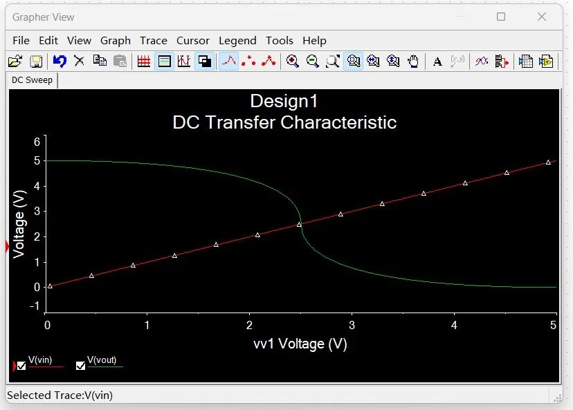
The ideal VTC of an inverter will present a steep step at 1/2Vin. Considering that we set the driving voltage to 5 V, we can obtain the ideal VTC shown in the figure below by adjusting the threshold voltages of PMOS and NMOS to -2.5 V and 2.5 V, respectively.