00
Introduction
NAND Flash is a type of non-volatile storage medium where charge is stored in a floating gate surrounded by an insulating layer, allowing it to retain stored data even when power is lost. It utilizes a “NOT-AND Gate” circuit structure, with storage cells connected in series. From smartphones to solid-state drives, it plays a crucial role in storing vast amounts of data due to its high speed, lightweight, and durability.

Basic Unit of NAND

01
Basic Unit
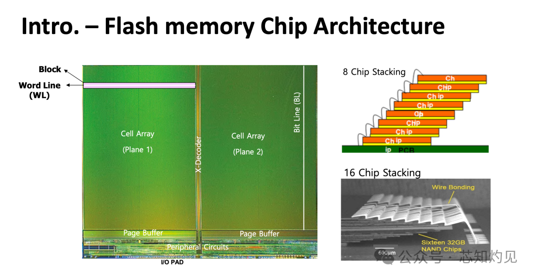
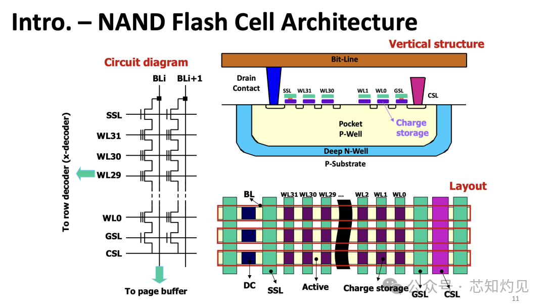
The basic unit structure of NAND Flash: Floating Gate Field Effect Transistor (FG FET). The architecture of NAND chips is ordered from large to small: Chip ➱ Die/LUN ➱ Plane ➱ Block ➱ Page ➱ Cell (FG FET).
Floating Gate Transistor
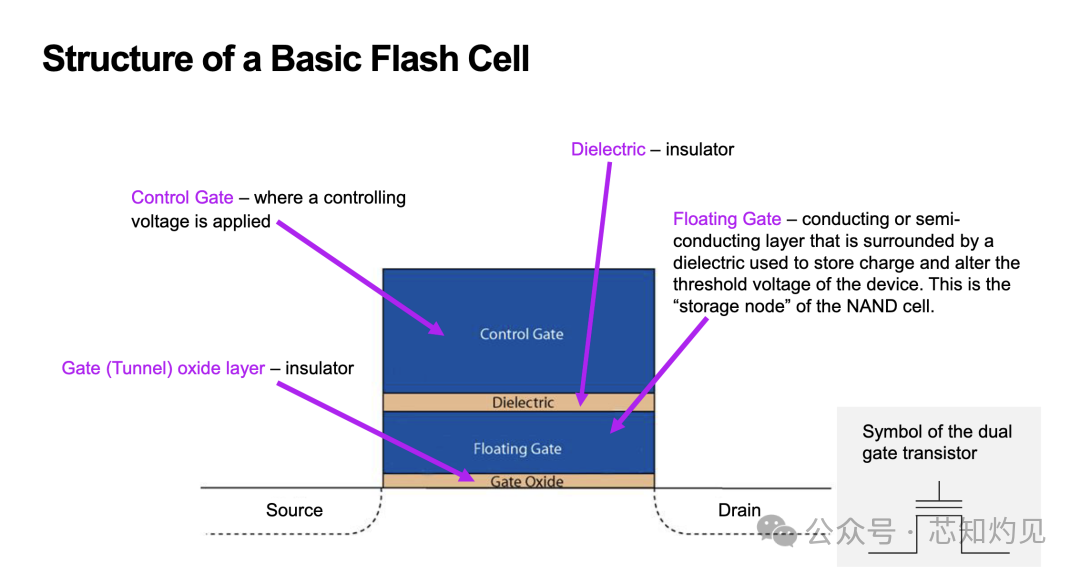
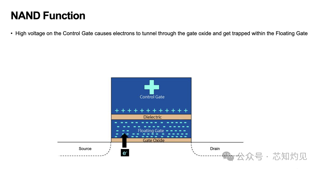
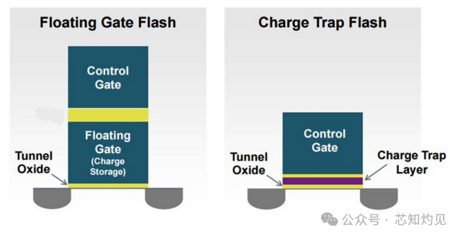
The floating gate transistor has five terminal electrodes: Bulk, Source, Drain, Control Gate, and Floating Gate. The first four terminal electrodes function similarly to a MOSFET, while the FG is used to determine “0” and “1” based on the amount of stored charge. Under high positive voltage, electrons tunnel through the Tunnel Oxide Layer, getting captured and stored in the FG.
Floating Gate vs Charge Trap
FG Flash uses conductive Poly-Si to store charge, allowing electrons to move freely within it.
CT Flash uses high trap density materials like Si3N4 to capture charge, making it difficult for electrons to move.

02
Operating Principles
NAND Flash achieves data storage through operations such as Erase, Write/Program, and Read.
Erase Operation
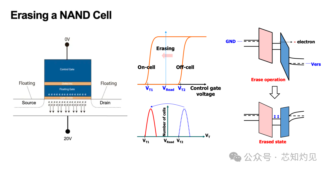
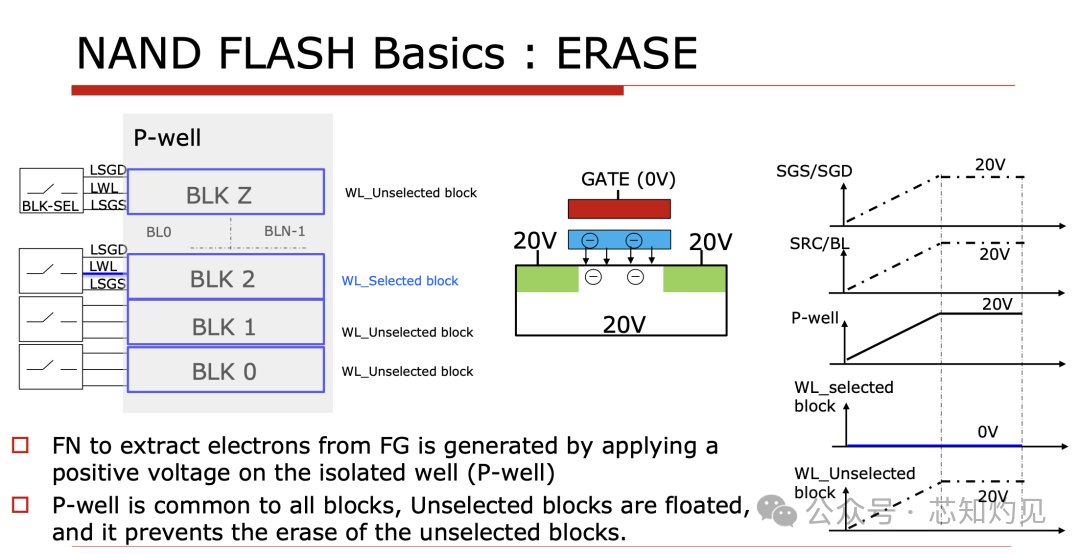
The erase operation applies high voltage to the Bulk, causing electrons to tunnel from the FG into the substrate via Fowler-Nordheim tunneling, changing the state from 1 to 0. CT Flash achieves this through direct tunneling without requiring a high electric field. Since electron tunneling can damage the Gate/Tunnel oxide layer, the erase operation is performed at the Block level.
Write Operation
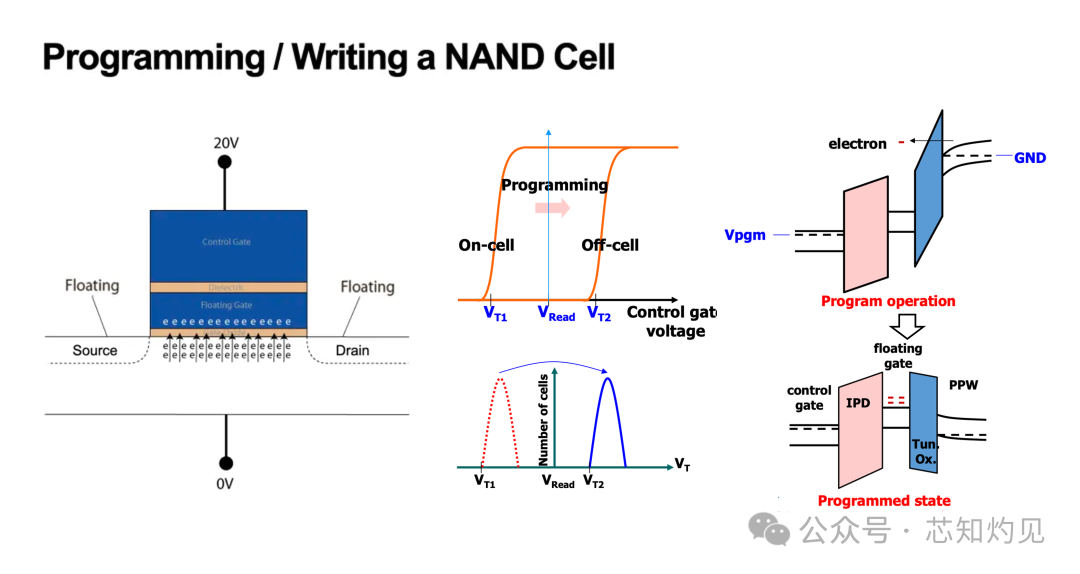
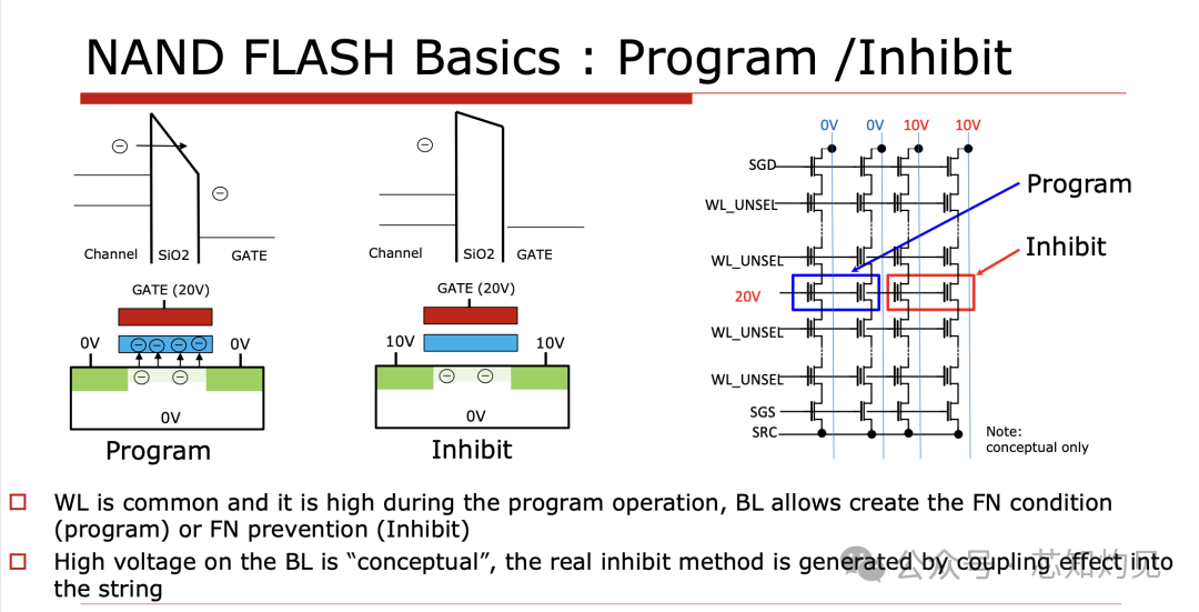
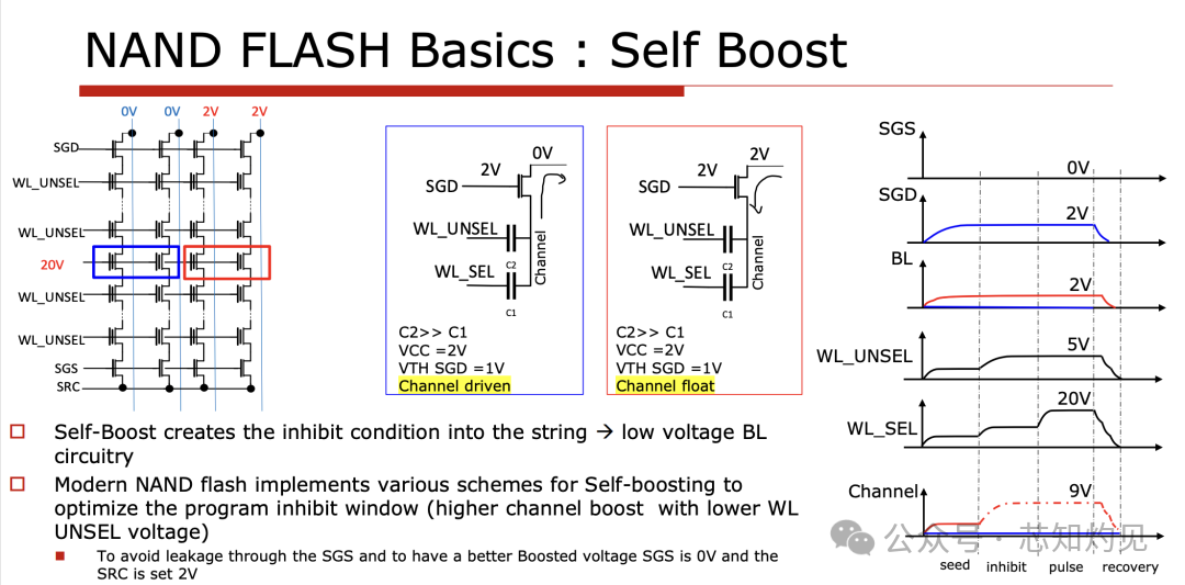
The write operation applies high positive voltage to the CG, causing electrons to tunnel from the Source into the FG via F-N tunneling, changing the state from 0 to 1. Before the write operation, data/charge in the FG must be erased. Similarly, the write operation is performed at the Page level.
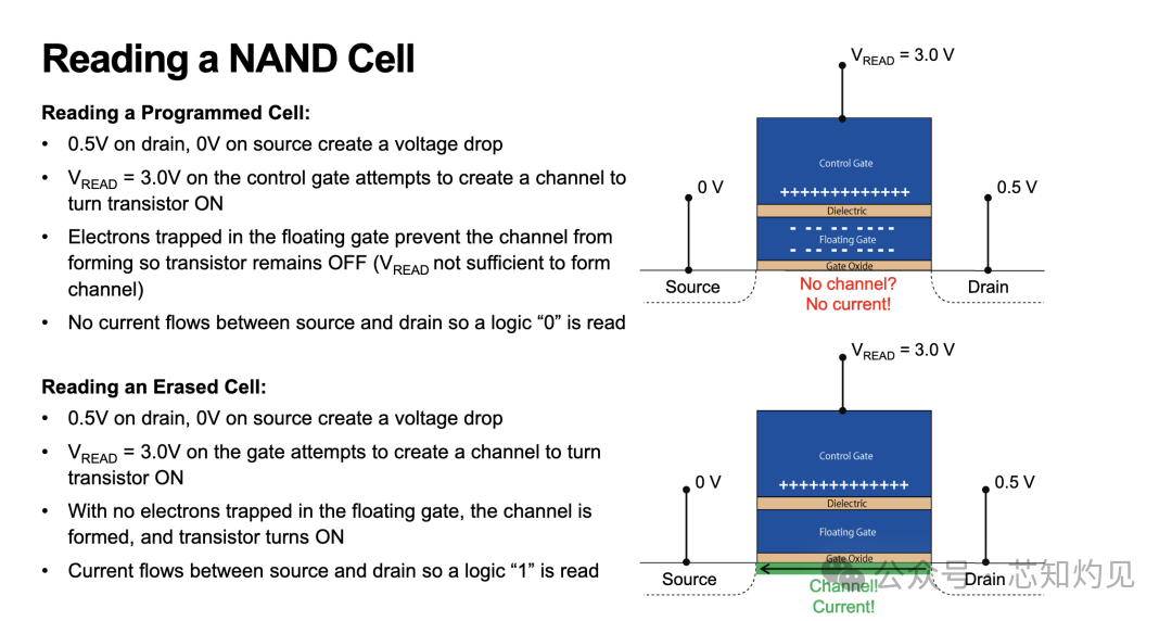
Read Operation
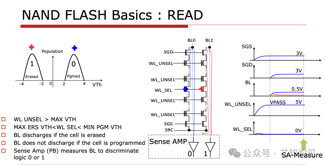
The read operation applies a small voltage to the CG, not altering the charge in the FG; when there is charge in the FG, no conductive channel exists between the Source and Drain, resulting in a readout of “0” at the Drain; when there is no charge in the FG, a conductive channel exists between the Source and Drain, resulting in a readout of “1” at the Drain.

NAND Architecture Evolution

01
2D NAND ➱ 3D NAND
In 1988, Toshiba first introduced NAND Flash, emphasizing lower cost per bit and higher performance. At the 1Z (~15nm, WL Half-Pitch) node, due to array reliability and electrostatic interference issues, planar 2D NAND reached its limits. To increase storage density and optimize performance, Samsung first mass-produced 3D NAND (V-NAND) in 2012, which involved vertically stacking storage cells.

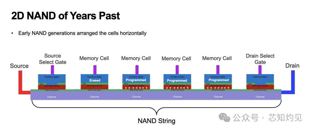
Early 2D NAND
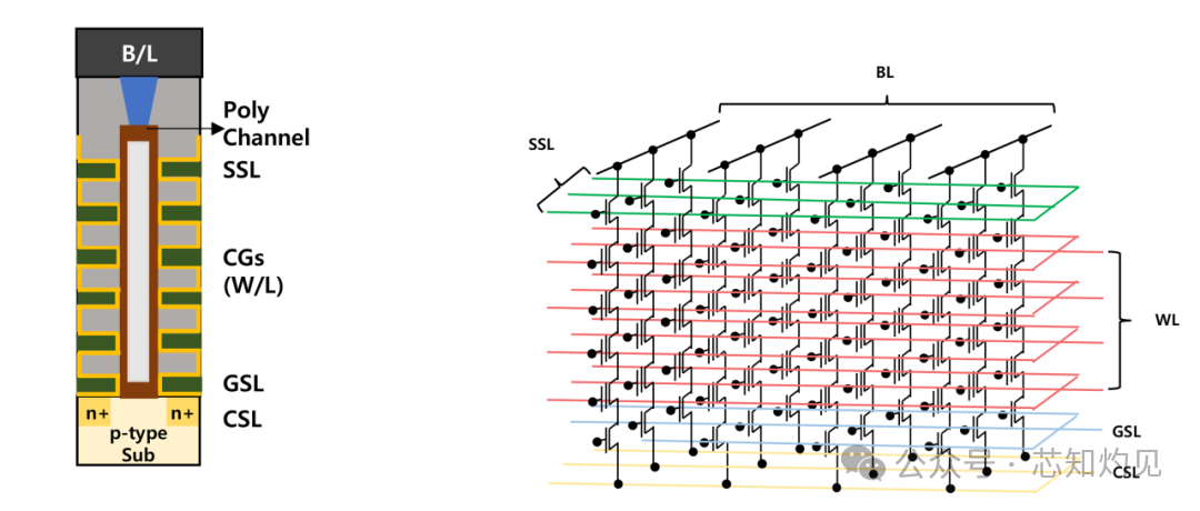
NAND uses a String structure, with multiple CELLS connected in series. The Source end connects to the Ground Select Line (GSL) for grounding control, enabling pathways during read operations; the Drain end connects to the String Select Line (SSL) to control whether to isolate this String.
3D NAND
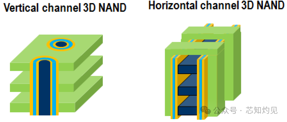
The array architecture in 3D NAND Flash mainly has two types: gate stacking and channel stacking.
Gate Stacking:Vertical channels with all-around gate structure, where current flows vertically. This structure is commonly used in commercial products.
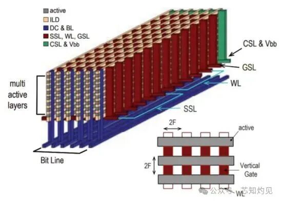
Channel Stacking:Horizontal channels where current flows laterally. Disadvantage: limited by the thickness of the tunneling oxide layer (ONO) in the BL spacing.
Program, Read & Erase Operations of 3D NAND
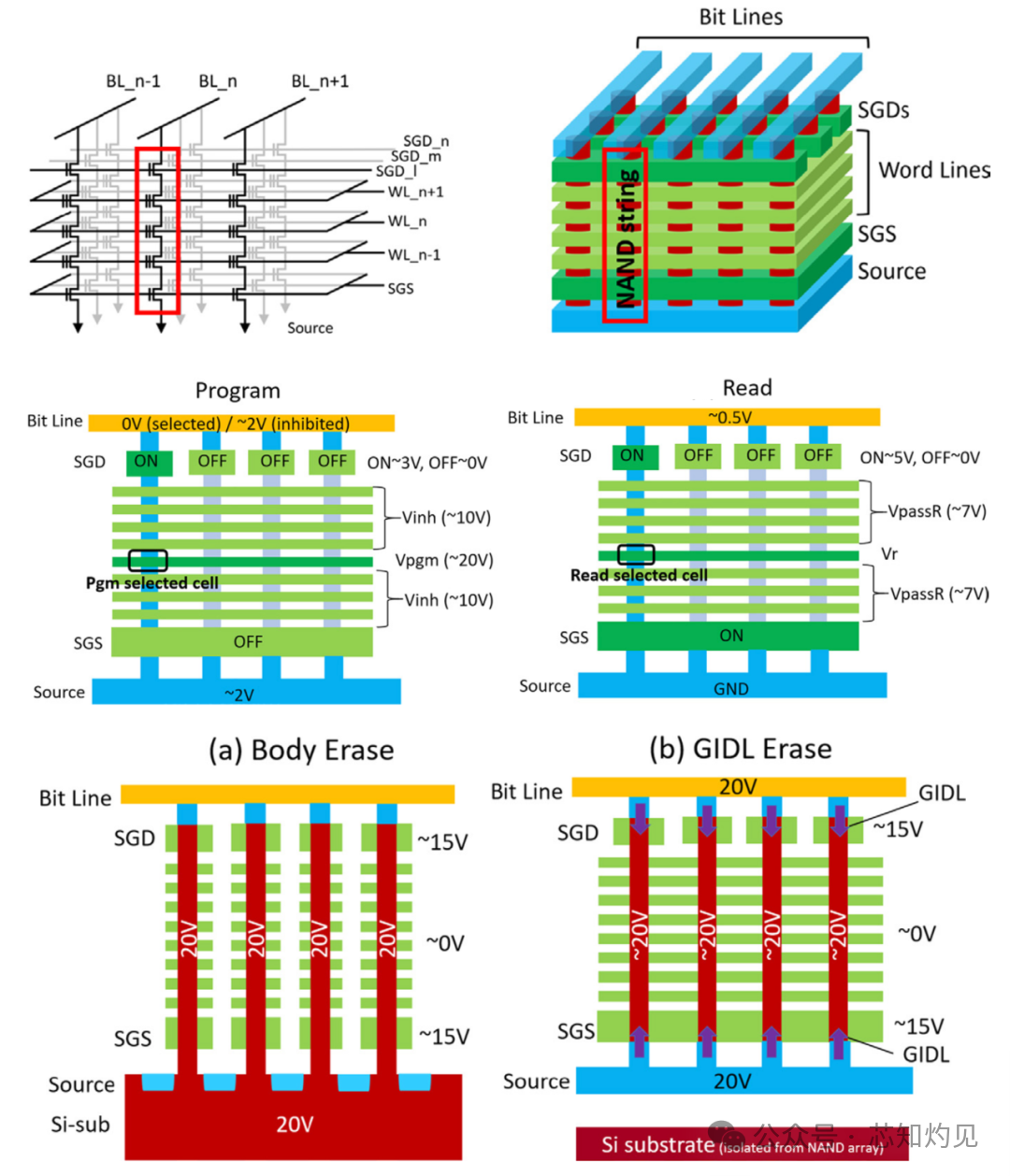
For 2D NAND, the channel uses single crystal silicon, with one SGD (Select Gate) at the Drain end of a Block; for 3D NAND, the channel is Poly-Si, with multiple SGDs in a Block to connect multiple strings and decode, introducing selection and deselection SGDs.
1. Program:Select a String connected to an SGD for writing (CG applies 20V), while other SGDs connected to that Block prohibit writing (CG applies 10V).
2. Read:Select a String connected to an SGD for reading, while other SGDs connected to that Block prohibit reading (CG applies 7V).
3. Erase:Erasure can be done in two ways: bulk erase and GIDL erase.
(a) Bulk Erase:Similar to 2D NAND, it requires applying positive voltage to the Si bulk and providing holes, allowing electrons in the FG to tunnel into the bulk.
(b) GIDL Erase:Since the string is separated from the Si bulk, the bulk cannot provide holes. Applying 20V to S and D, and 15V to SGS and SGD, generates electron-hole pairs in the PN junction of SGS and SGD, providing holes to the string, allowing electrons in the FG to tunnel out.
02
Evolution of 3D NAND Architecture
Both gate stacking and channel stacking have achieved the evolution from planar to three-dimensional structures. Gate stacking is characterized by vertical channels, evolving from Gate-First to Gate-Last processes, moving towards higher stacking layers and finer process nodes. Channel stacking maintains advantages in unit performance, but inter-layer connection complexity and selection line explosion have become limiting issues.
Evolution of NAND Architecture in Gate Stacking
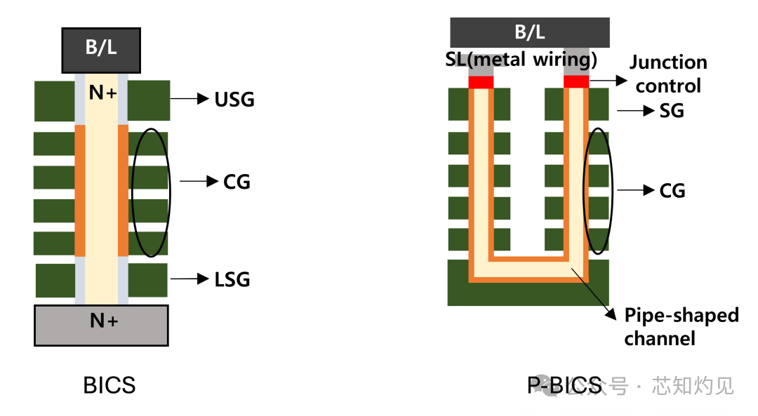
1. BiCS (Bit Cost Scalable):Utilizes Gate-First process to achieve high-density storage through vertically stacked gate layers. However, its linear String design faces issues like high source line resistance and limited reliability.
2. P-BiCS (Pipe BiCS):Introduces U-shaped String design, effectively reducing source line resistance and improving retention characteristics. Its unique pipe connection design significantly enhances performance.
3. TCAT (Transistor Cell Array Technology):Utilizes Gate-Last process, employing metal CG, supporting bulk erase operations. The equivalent circuit of this structure is akin to a 90-degree rotated planar NAND array.
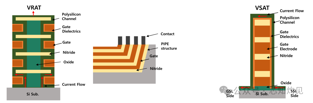
4. VRAT (Vertical Recessed Array Transistor):Introduces planar integration technology, improving WL interconnection efficiency.
5. VSAT (Vertical Stacked Array Transistor):Utilizes Gate-First process, simplifying the manufacturing process.
Evolution of NAND Architecture in Channel Stacking
1. VG NAND:Channel horizontally stacked, maintaining an effective cell size of 4F², supporting bulk erase operations, but requiring a large number of String select lines for addressing.
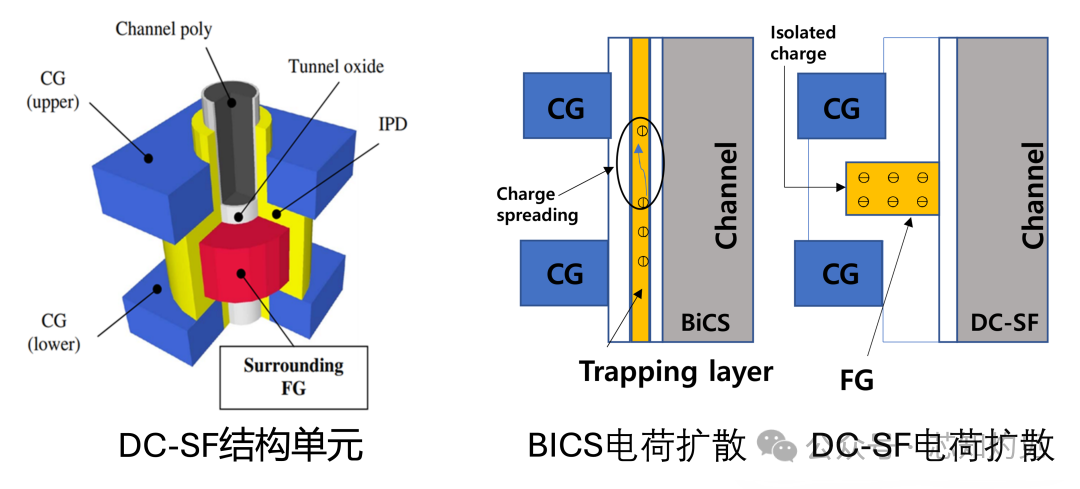
2. DC-SF (Dual Control Gate Surrounding Floating Gate):Utilizes FG as the charge storage layer, effectively preventing charge diffusion, with advantages of wide Program/Erase window and low operating voltage.
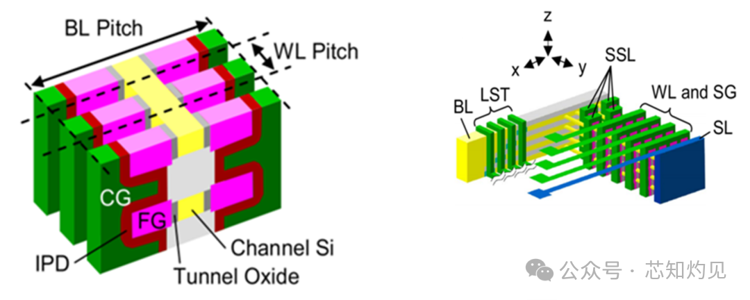
3. HC-FG (Horizontal Channel Floating Gate):Features stacked horizontal channels, combined with Layer Select Transistor (LST), achieving low-cost three-dimensional integration, compatible with traditional two-dimensional planar flash array processes.
03
3D NAND Scaling
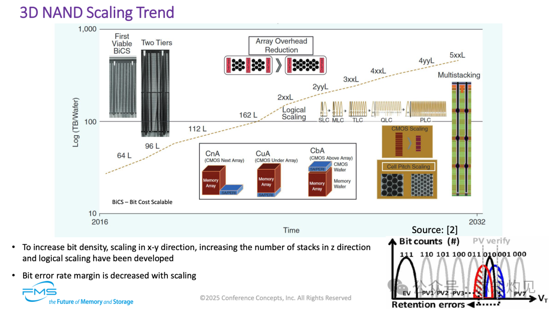
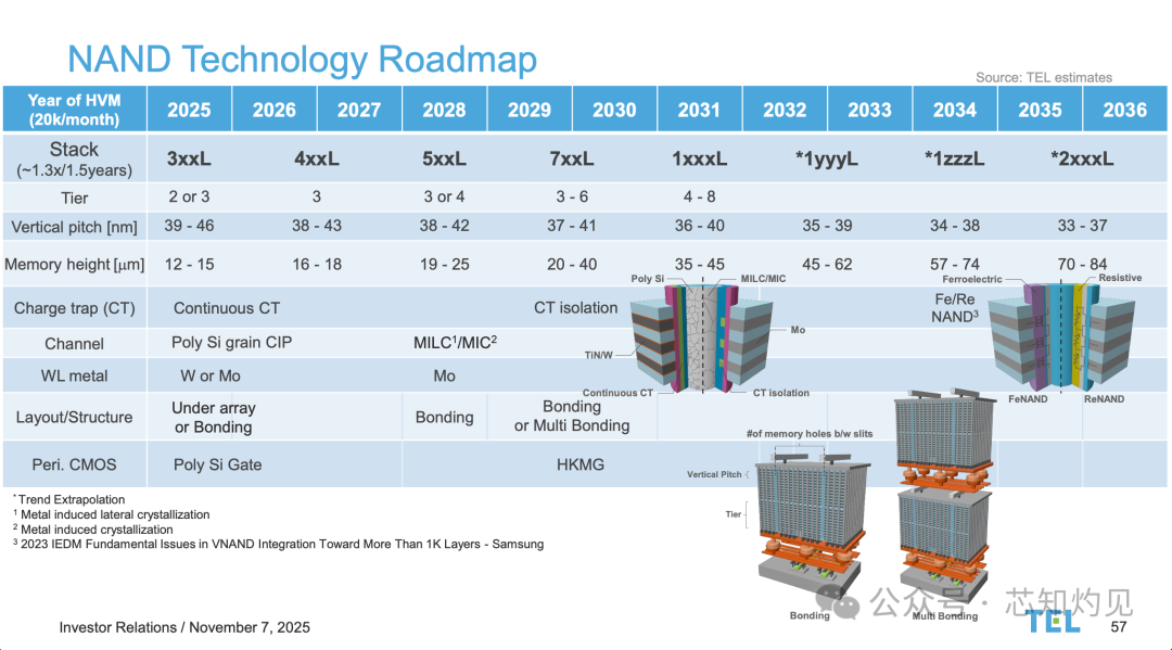
3D NAND scaling is achieved by stacking WL layers, increasing the height of NAND Strings. Challenges faced include: 1. Increased process complexity and costs; 2. Increased String height leading to reduced unit current; 3. NAND unit scaling resulting in smaller areas for CMOS in CuA structures. To address these challenges, further scaling in both lateral and vertical directions is needed.
Lateral Scaling
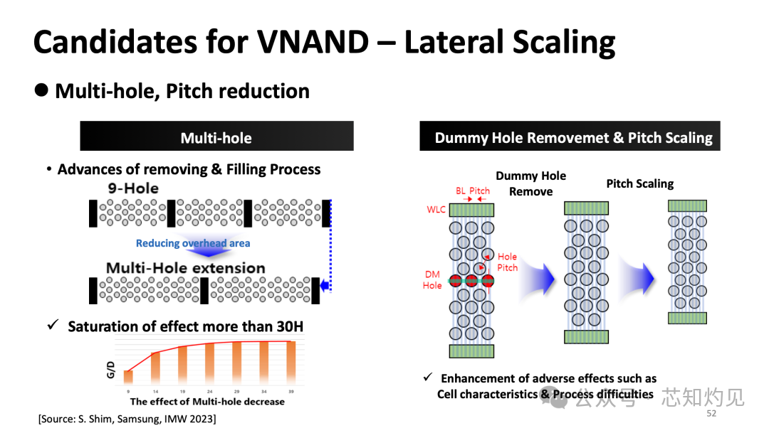
Reduce the number of Overhead areas, Slits, and Dummy Holes.
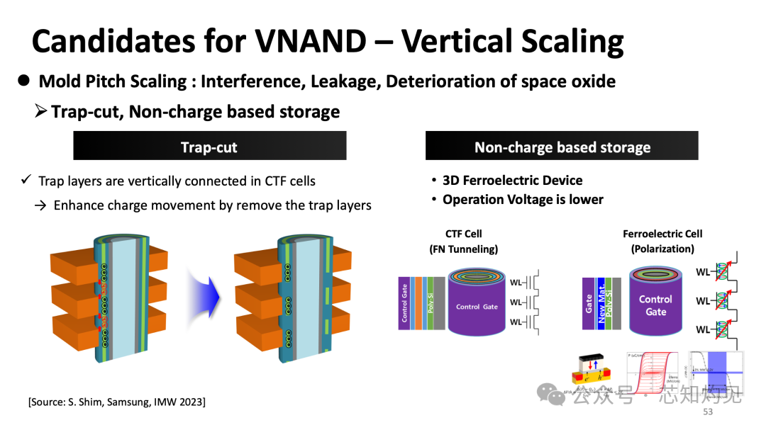
Vertical Scaling
• Increase the number of stacking layers
• CT isolation
• Ferroelectric devices
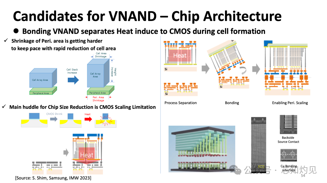
Chip Architecture Scaling
• CnA (CMOS next Array):Separates CMOS circuits and Array on a 2D plane, but increases area occupation.
• CuA (CMOS Under Array):Places CMOS circuits beneath the Array, reducing Die area.
• Xtacking®:Places CMOS above the Array, with CMOS and Array designed and manufactured on two separate wafers, then bonded together.
•Multi-Bonding:Multiple Cell structures bonded together.
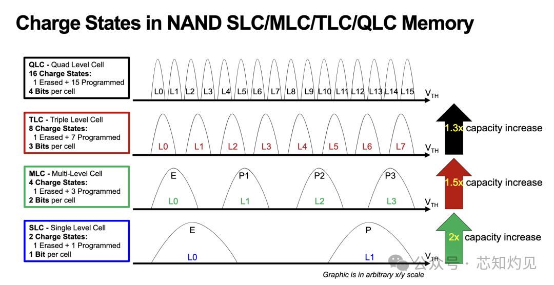
Logical Scaling
• SLC: 1 bit per cell (Single Level Cell)
• MLC: 2 bits per cell (Multi Level Cell)
• TLC: 3 bits per cell (Triple Level Cell)
• QLC: 4 bits per cell (Quad Level Cell)
• PLC: 5 bits per cell (Penta Level Cell)

Challenges in 3D NAND Technology

01
3D NAND Process
The 3D NAND array area process is mainly divided into: manufacturing of vertical channel regions and manufacturing of stepped WL contact regions.
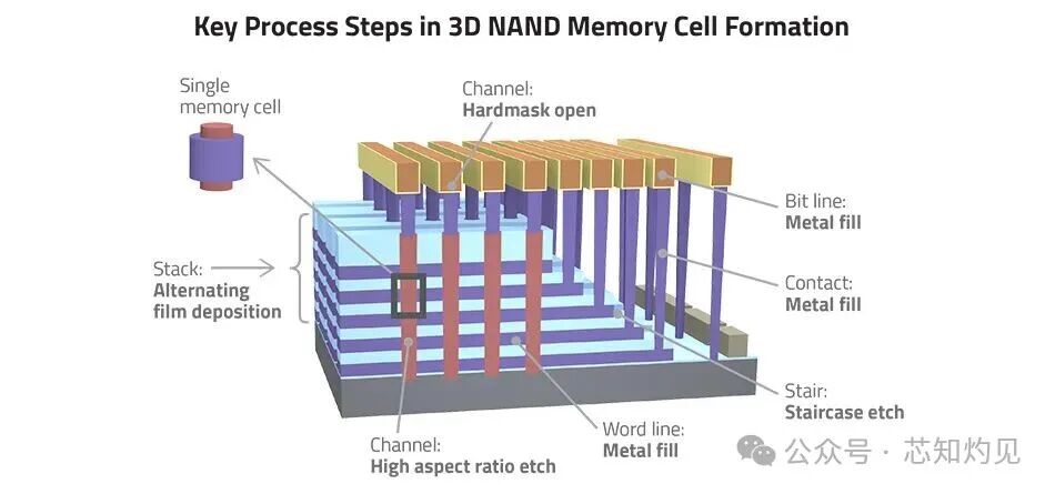
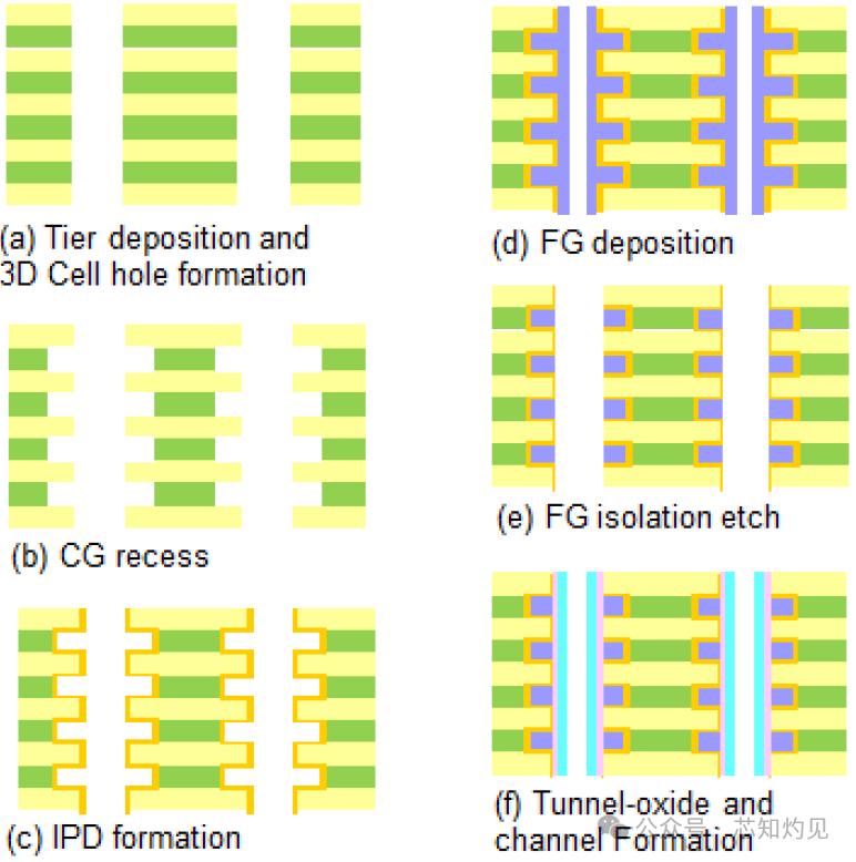
Gate First Process
a. Interleaved deposition of Poly-Si/Oxide, etching holes on multiple thin films;
b. Selective etching to recess the conductive layer;
c. Deposit interlayer dielectric IPD;
d. Deposit Poly-Si as FG;
e. Remove excess Poly-Si to isolate FG;
f. Deposit tunnel oxide layer and channel.
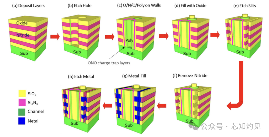
Gate Last Process
a. Deposit multiple layers of interleaved Oxide/Nitride;
b. Define the vertical channel region with a photolithography step and etch holes on multiple thin films;
c. Sequentially deposit Oxide (gate dielectric), Nitride (charge trapping), Oxide (tunneling dielectric), and Poly-Si channel, covering the sidewalls of the holes;
d. Fill the trench in the holes with Oxide;
e. Etch slits for cutting WL;
f. Remove the Nitride layer through chemical isotropic etching;
g. Fill the slits with metal;
h. Etch away excess metal.
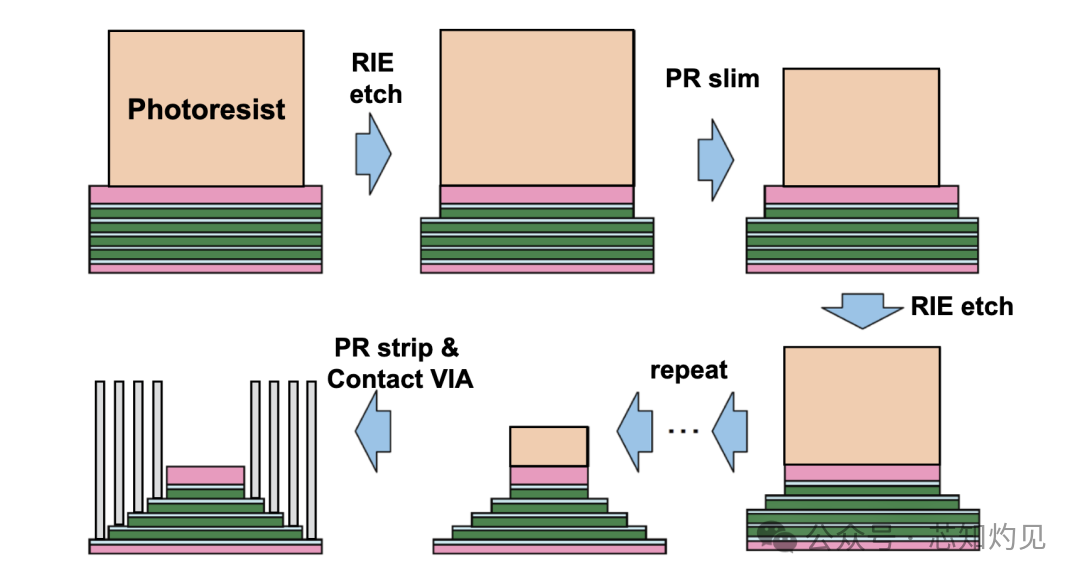
Etching of Stepped WL Contact Regions
Stepped WL is prepared through a single photoresist deposition, multiple photoresist trimming, and etching.
02
Process Challenges
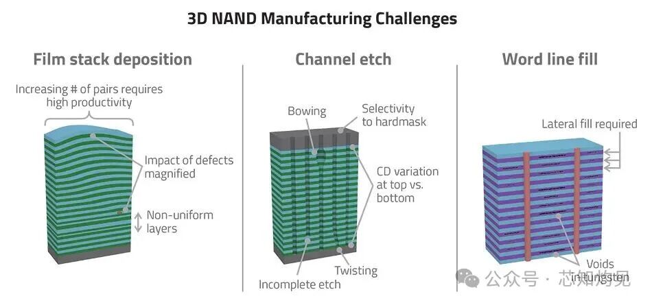
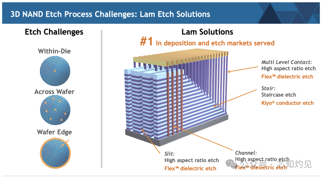
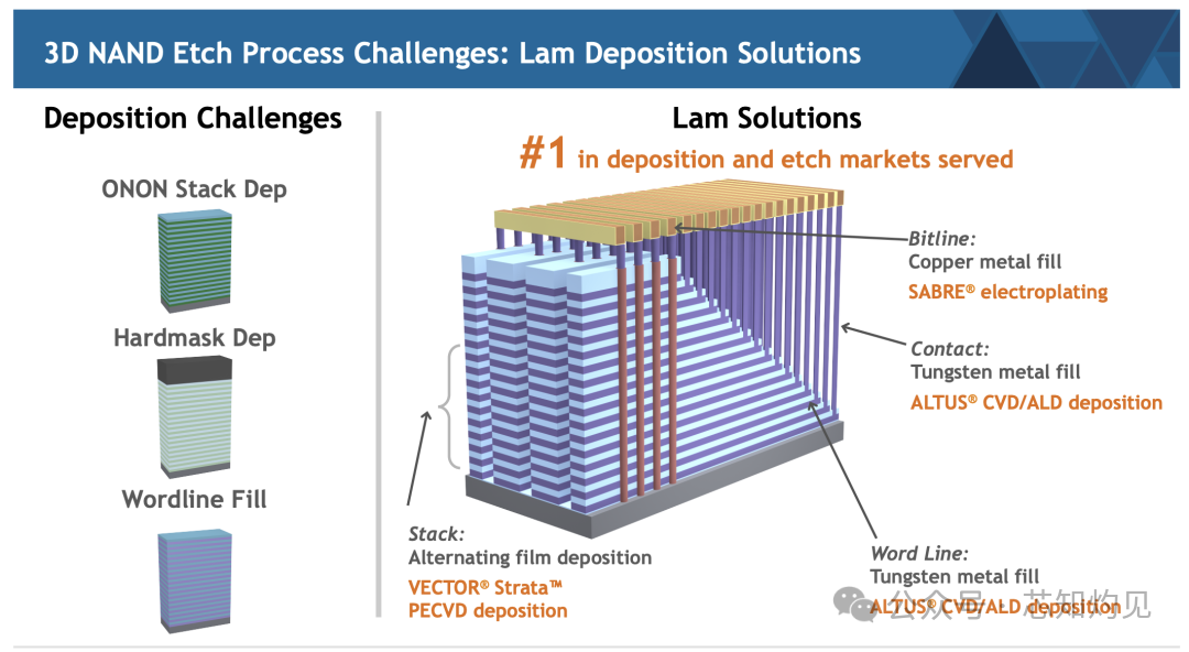
3D NAND requires controlling process variations in both horizontal and vertical directions, categorized into: High Aspect Ratio (HAR) etching and deposition.
HAR Etching
In planar NAND, the aspect ratio of holes is about 10:1, while in 3D NAND, the aspect ratio of holes is >40:1, making it difficult to control uniformity at the bottom and top.
Deposition
Layer stacking requires depositing multiple layers of Oxide/Nitride (ONON) or Oxide/Poly-Si (OPOP), necessitating control over uniformity, adhesion, and stress for each layer.
Material Aspects
WL resistance significantly increases with the number of layers, with the resistance in a 300-layer structure potentially reaching hundreds of ohms, affecting signal transmission speed. Next-generation WL materials are being explored using ruthenium or molybdenum to reduce resistivity.

Conclusion
SUMMARY
1. 3D NAND is undergoing continuous vertical stacking and horizontal architectural innovations to pursue higher storage density and lower costs.
2. Looking towards 2030, the entire industry is striving to achieve the goal of thousand-layer 3D NAND.
Reference
1.Inside NAND Flash Memories
2. 3D Flash Memories
3.Architecture and Process Integration Overview of 3D NAND Flash Technologies
4. https://thememoryguy.com
5. https://semiengineering.com/3d-nands-vertical-scaling-race/
6. Images sourced from the internet/agency analysis reports
⌛
Click the blue text to follow us
END