During the reflow soldering process, circuit boards are often prone to warping and bending. In severe cases, this can lead to issues such as cold solder joints and component misalignment. How can we overcome these challenges?
1. The Dangers of PCB Deformation
In automated surface mount lines, if the circuit board is not flat, it can lead to inaccurate positioning, making it impossible for components to be inserted or mounted onto the board’s holes and surface mount pads, potentially damaging the automatic insertion machine. After soldering, if the circuit board bends, it becomes difficult to trim the component leads evenly. Additionally, the board may not fit into the chassis or sockets, causing significant frustration for assembly factories. Current surface mount technology is advancing towards higher precision, speed, and intelligence, which places greater demands on the flatness of PCBs, the home for various components.
The IPC standard specifically states that the maximum allowable deformation for PCBs with surface mount devices is 0.75%, while for those without surface mount devices, it is 1.5%. In practice, to meet the demands for high precision and speed, some electronic assembly manufacturers have stricter requirements, with several clients requesting a maximum deformation of 0.5%, and in some cases, even 0.3%.
PCBs are composed of materials such as copper foil, resin, and glass cloth, each with different physical and chemical properties. When laminated together, residual thermal stress inevitably occurs, leading to deformation. Additionally, during the PCB manufacturing process, various procedures such as high temperatures, mechanical cutting, and wet processing can significantly impact board deformation. In summary, the causes of PCB deformation are complex and varied, and reducing or eliminating deformation due to material properties or processing has become one of the most complex challenges faced by PCB manufacturers.
2. Analysis of Causes of Deformation
The deformation of PCBs needs to be studied from several aspects, including materials, structure, pattern distribution, and processing. This article will analyze and elaborate on the various causes of deformation and improvement methods.
Uneven copper surface area on the circuit board can worsen warping and bending.
Typically, circuit boards are designed with large areas of copper foil for grounding purposes, and sometimes the Vcc layer also has large copper areas. When these large copper areas are not evenly distributed on the same circuit board, it can lead to uneven heat absorption and dissipation. The circuit board will expand and contract with temperature changes, and if these expansions and contractions do not occur simultaneously, it will create different stresses and cause deformation. If the board’s temperature reaches the Tg value limit, it will begin to soften, resulting in permanent deformation.
Connection points (vias) between layers of the circuit board can restrict expansion and contraction.
Modern circuit boards are mostly multilayered, and there are connection points (vias) between layers, which can limit the board’s ability to expand and contract, indirectly causing warping and bending.
The weight of the circuit board itself can cause it to sag and deform.
Typically, reflow ovens use chains to move the circuit boards through the oven, supporting the entire board at its edges. If there are excessively heavy components on the board or if the board is oversized, it can sag in the middle due to its own weight, causing bending.
The depth of V-Cut and connection strips can affect the deformation of the panel.
Essentially, V-Cut is a culprit that compromises the structural integrity of the board, as it involves cutting grooves into a large sheet of material, making it prone to deformation. (Related reading: PCB Edge Trimming – V-Cut Panel Cutting Machine)
2.1 Analysis of the Impact of Lamination Materials, Structure, and Patterns on Board Deformation
PCBs are laminated from core boards, prepregs, and outer copper foils. During lamination, the core board and copper foil undergo thermal deformation, and the amount of deformation depends on the coefficient of thermal expansion (CTE) of the two materials.
The CTE of copper foil is approximately  .
.
For standard FR-4 substrates, the Z-axis CTE below the Tg point is 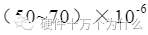 ; above the Tg point, it is (250~350)X10-6. The X-axis CTE is generally similar to that of copper foil due to the presence of glass cloth.
/*Note on Tg point:
High Tg printed circuit boards transition from a “glass state” to a “rubber state” when the temperature rises to a certain range, and this temperature is referred to as the glass transition temperature (Tg). In other words, Tg is the highest temperature (°C) at which the substrate maintains rigidity. At high temperatures, standard PCB substrate materials not only soften, deform, and melt but also exhibit a sharp decline in mechanical and electrical properties. Generally, Tg materials are above 130 degrees, high Tg is typically above 170 degrees, and medium Tg is around 150 degrees. PCBs with Tg ≥ 170°C are referred to as high Tg printed circuit boards. As the Tg of the substrate increases, the heat resistance, moisture resistance, chemical resistance, and stability of the printed circuit board improve. The higher the Tg value, the better the temperature resistance of the material, especially in lead-free processes where high Tg is more commonly used. High Tg refers to high heat resistance. With the rapid development of the electronics industry, especially in computer-related electronic products, there is a growing demand for PCB substrate materials with higher heat resistance as a crucial guarantee. The emergence and development of high-density mounting technologies represented by SMT and CMT have made PCBs increasingly reliant on the support of high heat resistance in terms of small aperture, fine line, and thinness. Therefore, the difference between standard FR-4 and high Tg FR-4 lies in their mechanical strength, dimensional stability, adhesion, moisture absorption, thermal decomposition, and thermal expansion characteristics under heat, especially after moisture absorption. High Tg products are significantly better than standard PCB substrate materials.
*/
The expansion of the core board with well-designed inner layer patterns varies due to differences in pattern distribution, core board thickness, or material properties. When the pattern distribution is uniform and the material types are consistent, deformation will not occur. However, when the lamination structure of the PCB is asymmetric or the pattern distribution is uneven, significant differences in CTE between different core boards can lead to deformation during lamination. The deformation mechanism can be explained by the following principles.
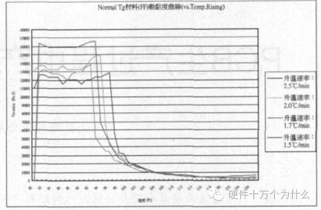
Figure 1: Dynamic viscosity curve of standard prepreg
Assuming there are two core boards with significantly different CTEs bonded together by prepreg, where core board A has a CTE of 1.5×10⁻⁵/°C and both core boards are 1000mm long. During the lamination process, the prepreg acts as the bonding layer, going through softening, flowing, filling the pattern, and curing stages to bond the two core boards together.
Figure 1 shows the dynamic viscosity curve of standard FR-4 resin at different heating rates. Generally, materials begin to flow around 90°C and start to crosslink and cure above the Tg point. Before curing, the prepreg is in a free state, and at this time, the core board and copper foil are in a state of free expansion due to heating, and the amount of deformation can be calculated based on their respective CTEs and temperature changes.
Simulating lamination conditions, with temperature rising from 30°C to 180°C,
the deformation amounts for the two core boards are
△LA=(180°C~30°C)x1.5×10-5m/°CX1000mm=2.25mm
△LB=(180°C~30°C)X2.5X10-5M/°CX1000mm=3.75mm
At this point, since the prepreg is still in a free state, the two core boards do not interfere with each other and have not yet deformed.
As shown in Figure 2, during lamination, the temperature is maintained for a period until the prepreg fully cures. At this point, the resin becomes solid and cannot flow freely, bonding the two core boards together. When the temperature decreases, if there is no interlayer resin constraint, the core boards would return to their initial lengths without deformation. However, in reality, the two core boards are bonded by the cured resin, and during the cooling process, they cannot freely contract. Core board A should contract by 3.75mm, but when the contraction exceeds 2.25mm, it will be hindered by core board A. To achieve force balance between the two core boards, core board B cannot contract to 3.75mm, while core board A’s contraction will exceed 2.25mm, causing the entire board to curve towards core board B, as shown in Figure 2.
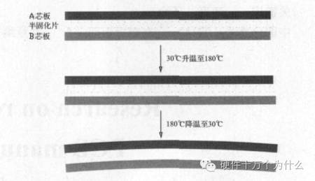
Figure 2: Deformation during lamination of core boards with different CTEs
From the above analysis, it can be seen that the lamination structure of the PCB, the type of materials, and whether the pattern distribution is uniform directly affect the CTE differences between different core boards and copper foils. The differences in expansion and contraction during the lamination process will be retained through the curing process of the prepreg and ultimately result in PCB deformation.
2.2 Deformation Caused by PCB Processing
The causes of deformation during PCB processing are complex and can be divided into thermal stress and mechanical stress. Thermal stress mainly arises during the lamination process, while mechanical stress is primarily generated during stacking, handling, and baking processes. Below is a brief discussion in order of the process.
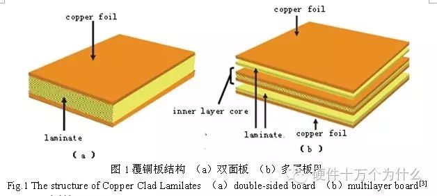
Incoming copper-clad laminates: Copper-clad laminates are generally double-sided boards with a symmetrical structure and no patterns. The CTE of copper foil and glass cloth is similar, so there is almost no deformation caused by CTE differences during lamination. However, the size of the copper-clad laminate press is large, and there are temperature differences in different areas of the heating plate, which can lead to slight differences in the curing speed and degree of resin in different areas during lamination. Additionally, the dynamic viscosity at different heating rates can vary significantly, leading to local stresses due to differences in the curing process. Generally, this stress will maintain balance after lamination but may gradually release and cause deformation during subsequent processing.
Lamination: The PCB lamination process is the main source of thermal stress, where deformation caused by material or structural differences has been analyzed in the previous section. Similar to copper-clad laminates, local stresses due to differences in the curing process will also occur, and due to the greater thickness, diverse pattern distribution, and more prepregs in PCBs, the thermal stress is more significant and harder to eliminate. The stresses present in the PCB will be released during subsequent drilling, shaping, or baking processes, leading to deformation.
Solder mask and character baking processes: Since solder mask inks cannot stack on top of each other during curing, PCBs are typically placed upright on racks for curing. The solder mask temperature is around 150°C, which is just above the Tg point of medium to low Tg materials. Above the Tg point, the resin is in a highly elastic state, making the board prone to deformation under its own weight or the strong airflow in the oven.
Hot air solder leveling: During standard hot air solder leveling, the solder pot temperature is between 225°C and 265°C, with a duration of 3 to 6 seconds. The hot air temperature is between 280°C and 300°C. During solder leveling, the board enters the solder pot at room temperature and undergoes post-treatment washing within two minutes after exiting. The entire hot air solder leveling process involves rapid heating and cooling. Due to the different materials of the circuit board and the uneven structure, thermal stress will inevitably occur during the heating and cooling process, leading to microscopic strain and overall deformation.
Storage: During the semi-finished stage, PCBs are generally inserted into racks. If the rack is improperly adjusted or if boards are stacked during storage, mechanical deformation can occur. This is especially severe for boards thinner than 2.0mm.
In addition to the above factors, there are many other influences on PCB deformation.
3. Improvement Measures
So how can we prevent warping and bending of the board during reflow soldering?
1. Reduce the impact of temperature on board stress
Since “temperature” is the main source of stress on the board, lowering the temperature of the reflow oven or slowing down the heating and cooling rates of the board in the reflow oven can significantly reduce the occurrence of warping and bending. However, there may be other side effects.
2. Use high Tg materials
Tg is the glass transition temperature, which is the temperature at which the material transitions from a glassy state to a rubbery state. Materials with lower Tg values begin to soften more quickly when entering the reflow oven, and the time spent in a rubbery state is longer, leading to more severe deformation. Using higher Tg materials can increase the board’s ability to withstand stress-induced deformation, but the cost of such materials is relatively higher.
3. Increase the thickness of the circuit board
Many electronic products aim for lightweight designs, resulting in board thicknesses of 1.0mm, 0.8mm, or even 0.6mm. Maintaining the board’s shape during reflow soldering at such thicknesses is quite challenging. It is recommended to use a thickness of at least 1.6mm if there are no strict requirements for thinness, as this can significantly reduce the risk of warping and deformation.
4. Reduce the size of the circuit board and the number of panels
Since most reflow ovens use chains to move circuit boards, larger boards can sag due to their own weight during the reflow process. Therefore, it is advisable to place the long edge of the board along the chain direction in the reflow oven to reduce sagging deformation caused by the board’s weight. Reducing the number of panels is based on the same reasoning; that is, during the reflow process, it is better to orient the narrow edge vertically to achieve the minimum sagging deformation.
5. Use reflow carrier templates
If the above methods are difficult to implement, the last resort is to use reflow carriers/templates to reduce deformation. Reflow carriers can minimize warping and bending because they help stabilize the circuit board during thermal expansion and contraction, ensuring that the board maintains its dimensions until the temperature drops below the Tg value and it hardens again.
If a single-layer carrier does not sufficiently reduce the deformation of the circuit board, a second layer can be added to sandwich the board between two carriers, significantly reducing the deformation during reflow. However, these carriers can be quite expensive and require additional labor for placement and retrieval.
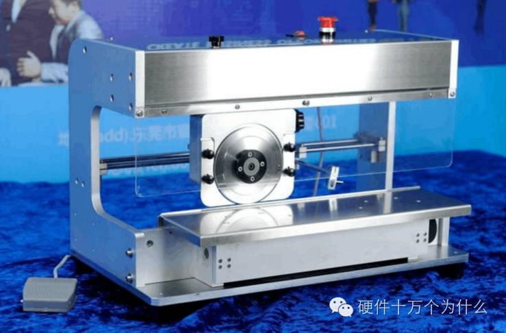
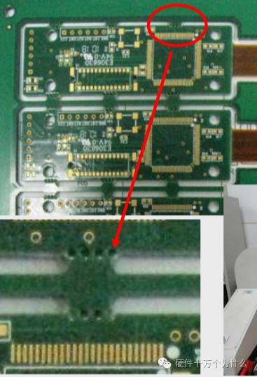
6. Replace V-Cut with solid connections or stamp holes for panel separation
Since V-Cut compromises the structural strength of the panel, it is advisable to avoid using V-Cut for panel separation or to reduce the depth of the V-Cut.
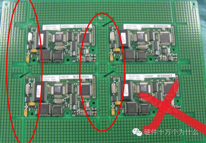
Solid connection: Using a knife-type panel cutting machine
Stamp holes
Optimization in PCB Production Engineering:
Impact of Different Materials on Board Deformation
Statistics on the defect rate of deformation exceeding standards for different materials are shown in Table 1.
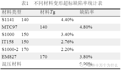
From the table, it can be seen that the defect rate for deformation in low Tg materials is higher than that in high Tg materials. The high Tg materials listed in the table are all filled materials with a CTE less than that of low Tg materials. Additionally, during subsequent processing after lamination, the maximum baking temperature of 150°C will have a greater impact on low Tg materials than on medium to high Tg materials.
Engineering Design Research
Engineering design should avoid asymmetric structures, materials, and patterns to reduce deformation. During the research process, it was also found that core board lamination structures are more prone to deformation than copper foil lamination structures. Table 2 shows the test results for two types of structural boards.
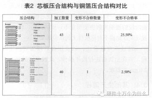
From Table 2, it can be seen that there is a significant difference in the defect rates of deformation between the two structures. This can be understood as the core board lamination structure consists of three core boards, making the expansion and contraction and stress changes between different core boards more complex and harder to eliminate.
In engineering design, the form of the panel frame also has a significant impact on deformation. Generally, PCB factories have continuous large copper skin frames and non-continuous copper dot or block frames, which have different effects.
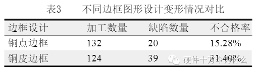
Table 3 shows the comparative test results for two types of frame designs. The reason for the different deformation performances of the two frame types is that the continuous copper skin frame has higher strength, resulting in greater rigidity during lamination and panel processing, making it harder for residual stresses within the board to release. This stress is concentrated and released after shaping, leading to more severe deformation. In contrast, the non-continuous copper dot frame gradually releases stress during lamination and subsequent processing, resulting in less deformation after shaping.
The above are some possible influencing factors related to engineering design. If these can be flexibly applied during design, the impact of deformation due to design can be reduced.
3.3 Lamination Research
Lamination has a crucial impact on deformation. By setting reasonable parameters, selecting appropriate presses, and using proper stacking methods, stress generation can be effectively reduced. For generally symmetrical structural boards, it is important to ensure symmetrical stacking during lamination and to symmetrically place tooling boards, cushioning materials, and other auxiliary tools. Additionally, using a hot and cold integrated press can significantly help reduce thermal stress. The reason is that a hot and cold separate press transfers the board to the cold press at high temperatures (above GT temperature), causing the material to lose pressure and rapidly cool, which can lead to rapid release of thermal stress and deformation. In contrast, a hot and cold integrated press can achieve a gradual cooling process at the end of hot pressing, avoiding loss of pressure at high temperatures.
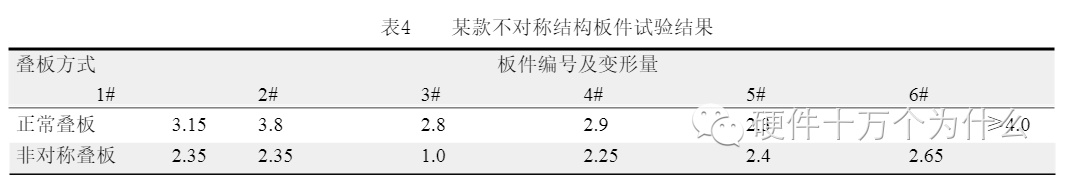
Moreover, for special customer requirements, there will inevitably be some materials or structures that are asymmetric. In such cases, the deformation caused by differences in CTE, as analyzed earlier, will be very pronounced. To address this issue, we can attempt to use asymmetric stacking methods, where the principle is to use asymmetrically placed cushioning materials to achieve different heating rates on both sides of the PCB, thereby affecting the expansion and contraction of different CTE core boards during heating and cooling stages to resolve inconsistent deformation. Table 4 shows the test results for a certain asymmetric structural board from our company.
By using asymmetric stacking methods, increasing post-curing processes, and performing leveling operations before shipment, this board ultimately met the customer’s requirement of 2.0mm.
3.4 Other Production Processes
In PCB production processes, in addition to lamination, there are several high-temperature treatment processes such as solder mask, character printing, and hot air leveling. The maximum temperature during solder mask and character baking processes is 150°C, which, as mentioned earlier, is above the Tg point for standard Tg materials. At this temperature, the material is in a highly elastic state and can easily deform under external forces. Therefore, it is important to avoid stacking boards during baking to prevent the lower boards from bending. Additionally, during baking, the direction of the boards should be parallel to the airflow.
During hot air leveling processing, it is essential to ensure that the boards are laid flat for at least 30 seconds after exiting the solder pot to avoid sudden cooling from post-treatment washing causing deformation.
In addition to production processes, the storage of PCB boards at various stations also has a certain impact on deformation. In some manufacturers, due to excessive waiting for production and limited space, multiple racks of boards are stacked together for storage, which can lead to mechanical deformation. Since PCBs have a certain degree of plasticity, these deformations may not fully recover during subsequent leveling processes.
3.5 Pre-shipment Leveling
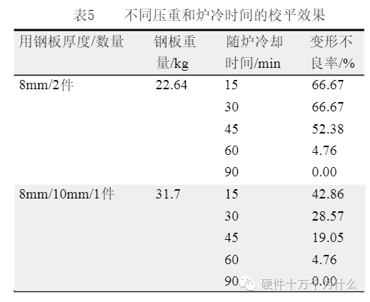
Most PCB manufacturers have a leveling process before shipment. This is because deformation caused by heat or mechanical forces is unavoidable during processing. Mechanical leveling or thermal leveling before shipment can effectively improve this. Due to the heat resistance of solder masks and surface coatings, the baking temperature is generally kept below 140°C to 150°C, which is just above the Tg temperature of standard materials. This is very beneficial for leveling standard boards, while the leveling effect on high Tg materials is not as significant. Therefore, for individual severely warped high Tg boards, the baking temperature can be slightly increased, but care must be taken regarding the quality of inks and coatings. Additionally, using weights during baking and increasing the cooling time after the oven can also improve deformation. Table 5 shows the test results of different weights and cooling times on the leveling effect of boards, indicating that increasing weight and extending cooling time have a significant leveling effect on deformation.
Some content is reproduced from “Printed Circuit Information”, Author: Liu Hailong, Shenzhen South Circuit Co., Ltd.