01
Overview
The PIL module is an optional add-on for PSIM software. It provides Processor-in-the-Loop (PIL) simulation capabilities, where the power portion of the system is simulated in PSIM on a computer, while the rest of the system is implemented in C code running on DSP hardware. With the PIL module, you can easily test and validate control code, whether it is handwritten in PSIM or automatically generated, and verify it on actual DSP hardware through the power circuit simulated in PSIM.
PSIM offers two types of PIL modules: the general PIL model PIL Block and the dedicated PIL model PIL Block (InstaSPIN). The general PIL model can be used for general PIL simulations, while the dedicated PIL model PIL Block (InstaSPIN) can be used for both PIL simulation and code generation specifically for TI InstaSPIN motor control algorithms.
PIL Module: Interface module for PIL simulation.
PIL Module (InstaSPIN): Interface module for PIL simulation used for Texas Instruments’ InstaSPIN motor control algorithm.
02
Application Example
This tutorial details how to build and execute the PIL simulation process step by step using the general PIL model, with the main steps including:
Preparing the PIL simulation code
PSIM setup
Hardware setup
The following example illustrates this process using a buck converter, located in the PSIM installation directory under “examples\PIL\Buck Converter (F28335)”.
2.1. Preparing the PIL Simulation Code
The circuit schematic of the buck converter is shown below:
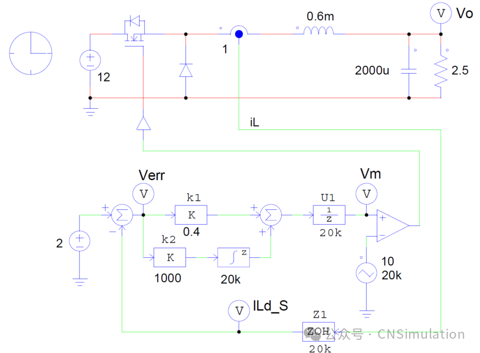
Figure 176, Circuit schematic of the BUCK converter
The buck converter uses average current mode control, with a switching frequency of 20 kHz, and the unit delay module U1 represents an inherent one-cycle delay in digital control.
The first step in the PIL simulation is to generate code, which can be either handwritten or automatically generated using PSIM’s SimCoder feature. This tutorial uses PSIM to automatically generate the code.
Generating Code
First, modify the circuit by adding an A/D converter after the current sensor, replacing the carrier and comparator with a PWM generator, and defining the hardware target board. For details on using SimCoder, refer to the tutorial “Tutorial – Auto Code Generation for F2833x Target.pdf”.
The A/D converter and PWM generator are models from PSIM’s F2833x Target library, simulating the functionality of the A/D converter and PWM generator in the F28335 DSP hardware. The modified circuit is shown below, with the A/D converter and PWM generator highlighted in yellow.
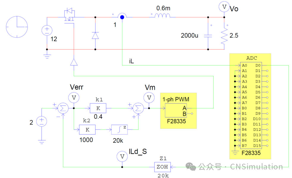
Figure 177, Circuit schematic of the buck converter for code generation
Note that the A/D converter has a built-in input limitation. If the input mode of the A/D converter is set to DC, the input limitation range is 0 to +3V; if the input mode is set to AC, the limitation range is -1.5V to +1.5V. When the input exceeds the limitation range, it will be forced to the boundary value. For example, if the input mode is set to DC, the input iL will be limited to 0 to +3V.
PSIM can simulate this circuit and automatically generate code that can run on DSP hardware. Click the menu Simulate >> Generate Code to create a subfolder named “buck converter (simcoder) (C code)” containing C code and other necessary files for CCS. Copy a duplicate of this subfolder and rename it to “buck converter (PIL) (C code)” for modifying the code for PIL simulation.
Modifying the PIL Simulation Code
After generating the code (either handwritten or PSIM-generated), the second step is to determine the interface variables between the code and PSIM. Using the PIL model as the interface, the interface variables include signals from PSIM (such as measured voltage or current) and signals sent to PSIM (such as PWM modulation signals). Below are some typical interface variables:
From PSIM: Output variables from the A/D converter;
Sent to PSIM: Input to the PWM generator, and any other internal variables used for display/debugging.
For example, in this case, the variable from PSIM is the output from the A/D converter, and the variable sent to PSIM is the modulation signal Vm at the input of the PWM generator. If you want to monitor the internal signal Verr, you can add Verr as an additional interface variable.
It is important to note that the output of the PWM generator cannot be used as an interface variable, as the output is a real PWM gate signal on the hardware output pin and cannot be sent directly to PSIM; the PWM gate signal needs to be generated through the circuit in PSIM.
Only two code modifications are needed:
All interface variables must be defined as global variables, initialized to 0;
The code statement assigning a value to the ADC output needs to be commented out, as there is no input on the actual ADC pins in the hardware, and the value of the interface variable must come from PSIM.
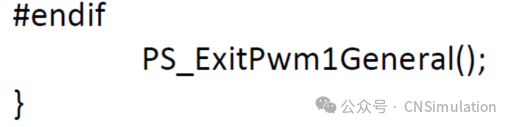
Below is the original interrupt service routine code from the “buck_converter__simcoder_.c” file (located in the subfolder “buck converter (simcoder) (C code)”) before modification:
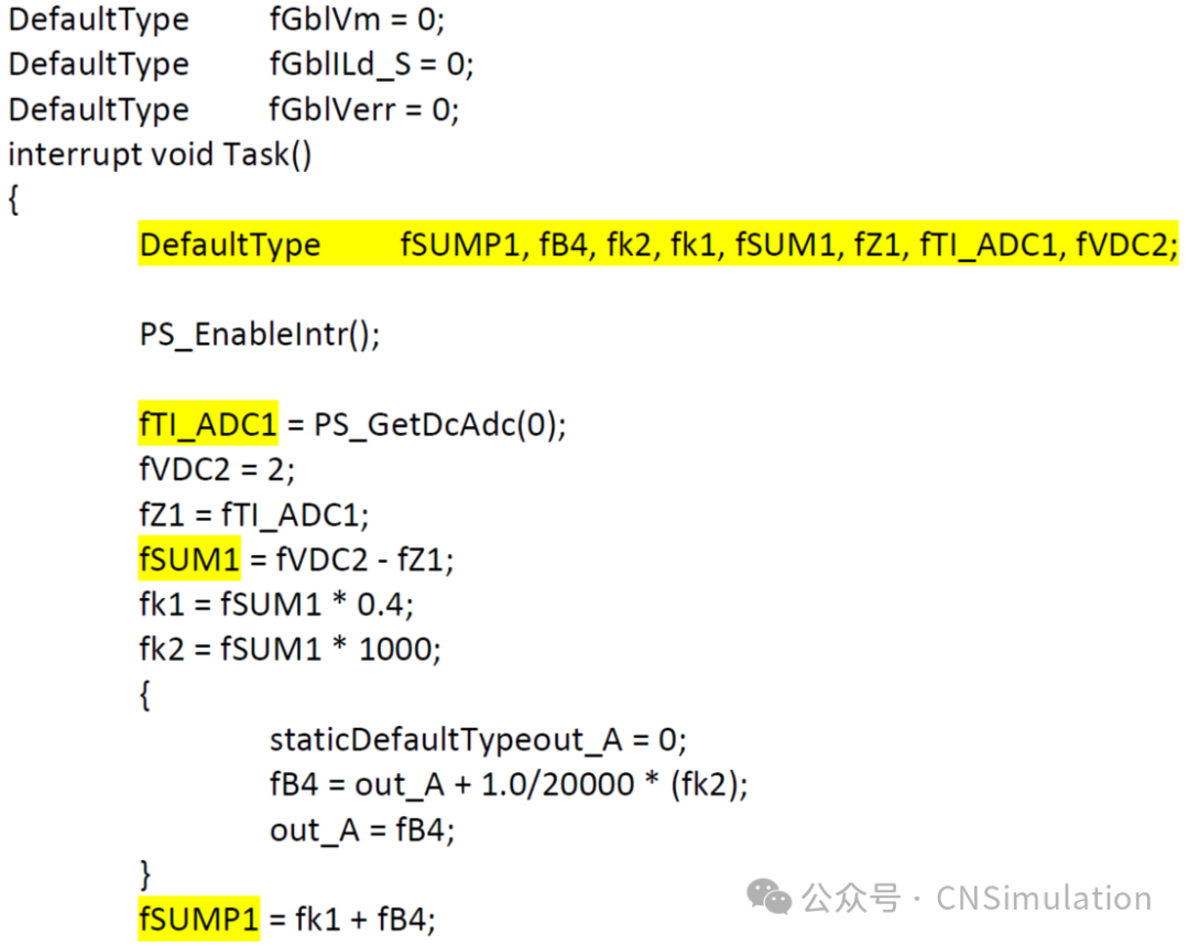
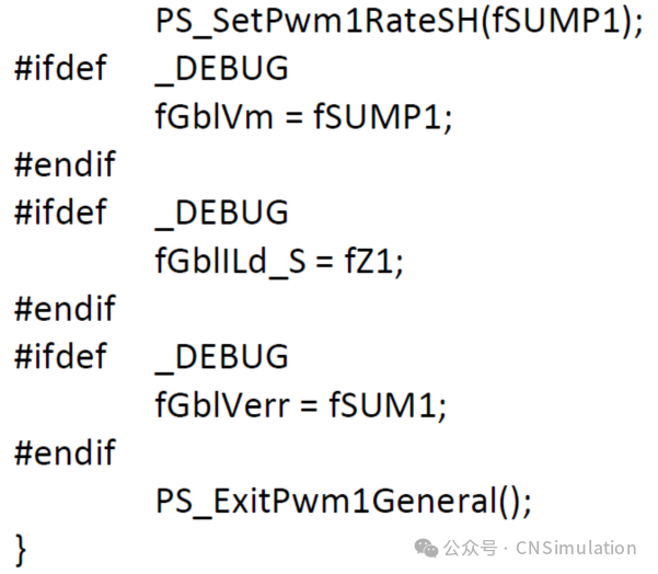
From the code, the interface variables can be identified: ADC output fTI_ADC1 and input to the PWM generator fSUMP1, with the error signal Verr highlighted in yellow as fSUM1.
Open the file “buck_converter__simcoder_.c” in the subfolder “buck converter (simcoder) (C code)” with a text editor, and make the modifications as described earlier, ensuring that the interface variables are initialized to 0. Below is the modified code.
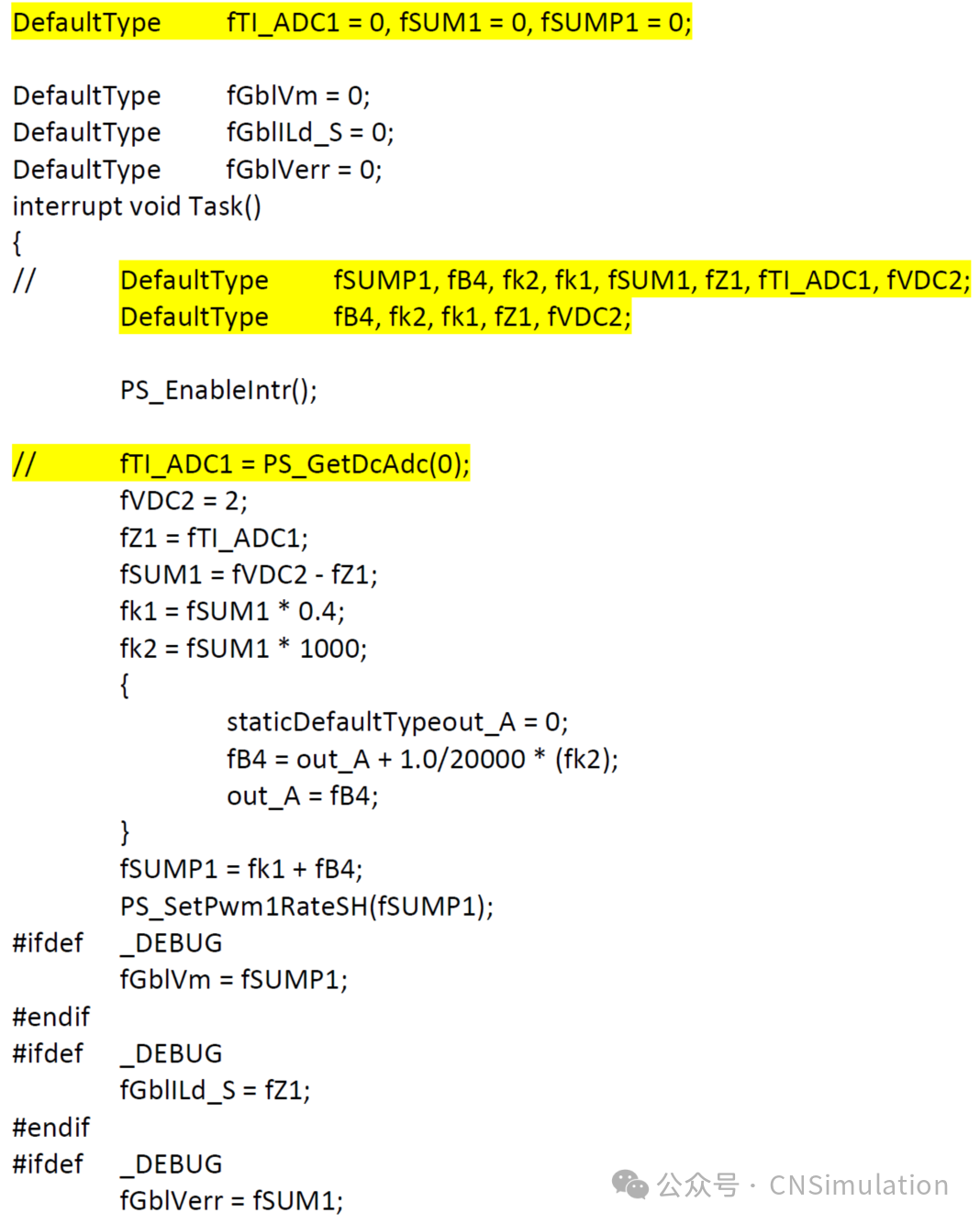
The lines of code highlighted in yellow are the modified parts, which are:
The variables fTI_ADC1, fSUM1, and fSUMP1 are defined as global variables, and their definitions inside the interrupt function have been removed;
The ADC variable fTI_ADC1 has been commented out.
Then compile the modified code. In CCS, click Project >> Import Legacy CCS v3.3 Project, and select the “buck_converter__simcoder_.pjt” file in the “buck converter (PIL) (C code)” folder. Note that the import of the previous CCS v3.3 project can only be done once; once converted to CCS v6.1 or higher, the project file can be opened directly even if the code has been modified.
In the CCS environment, click Project >> Build All to build the project, generating the hardware executable code “buck_converter__simcoder_.out” in the “buck converter (PIL) (C code)/RamDebug” folder. Note that the executable code can also be compiled in RAM and Flash.
2.2. Setting Up PSIM
To enable the schematic for PIL simulation, ensure that the CCS folder path is supported. If CCS v5 is installed at “c:\TI\ccsv5” or CCS v6 is installed at “c:\TI\ccsv6”, no action is needed, as PSIM already includes these two folder paths. If CCS is not installed in the above two folder paths, you need to add the CCS installation folder path to PSIM’s search path via Options >> Set Path.
Modify the previous circuit by removing the control circuit, except for the PWM generator and unit delay module U1, and replacing it with the PIL model (the PIL model is located in the model library under Elements >> Control >> PIL Module). The unit delay module is retained because the PIL model does not include any delay. Additionally, the input to the PIL must be limited to the range of 0 to 3V to simulate the built-in A/D converter’s clipping characteristics and prevent inputs from exceeding the specified range.
The modified circuit is shown below.
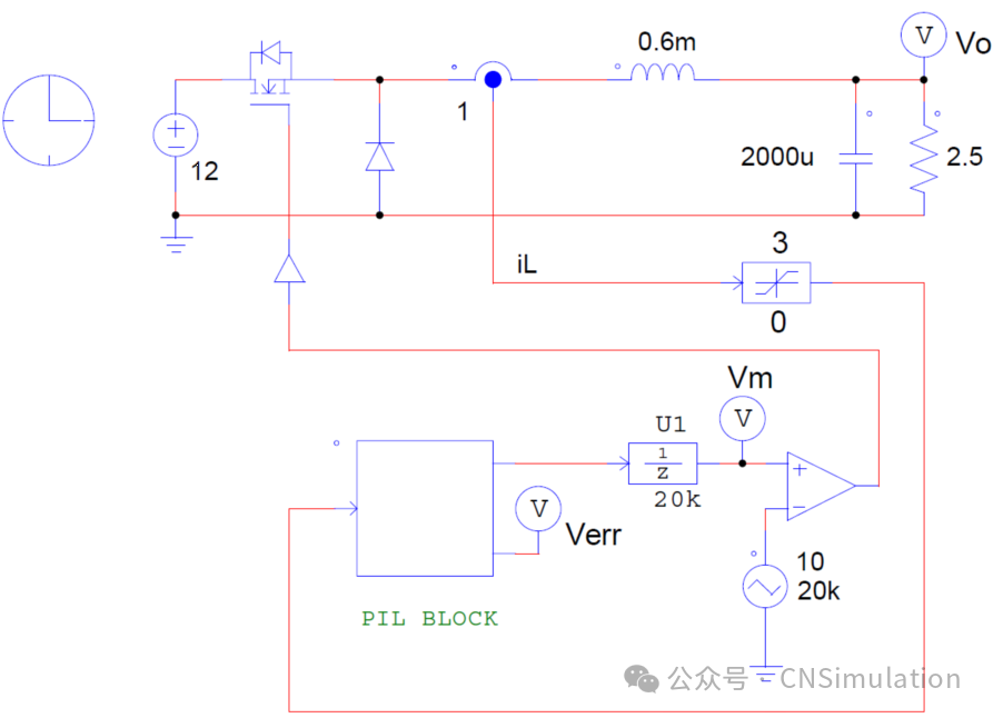
Figure 178, Modified circuit schematic for PIL simulation
In this example, the definition of the PIL module is as follows.

Figure 179, Definition of the PIL module
When the option Run Code Composer Studio in simulation is checked, you need to wait for CCS to start before running. Similarly, do not exit CCS during PIL simulation. If you need to debug code in CCS, click Simulate >> Pause Simulation in PSIM to pause the PIL simulation, and then perform step-by-step debugging in CCS. Note that while paused, the values passed to the DSP from PSIM remain unchanged; to resume simulation, click Simulate >> Restart Simulation in PSIM.
If you select Run Code Composer Studio in simulation and CCS does not start, but the Eclipse platform resource window appears, as shown below, you need to find Window >> Open Perspective, and select CCS Debug to open the CCS window.
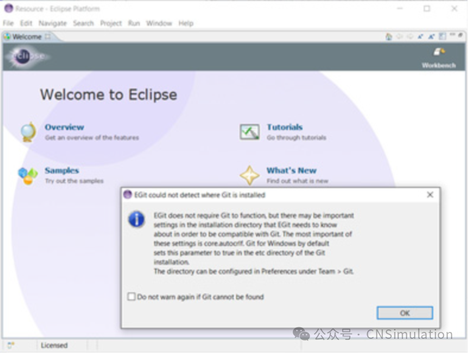
Figure 180, CCS startup interface
It is important to note that the PIL simulation with multiple sampling frequencies has not yet been validated. It is recommended that if you encounter multiple sampling frequencies, sample all input variables at the highest sampling frequency, and then reduce the sampling frequency of the selected variables after the ADC. For example, if there are two inputs, one at 10kHz and the other at 1kHz, sample both signals at 10kHz, and then use a zero-order hold to reduce the sampling frequency of the second signal to 1kHz.
2.3. Setting Up Hardware
The only hardware setup required for PIL simulation is to connect the controller hardware to the computer. In this example, the TI development kit is connected to the computer via a USB cable, as shown below.
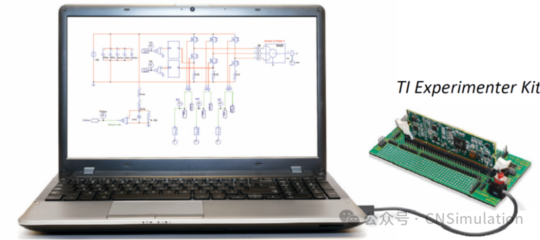
Figure 181, Hardware configuration for PIL
After connecting the controller hardware, click the menu Simulate >> Run Simulation in PSIM to run the simulation. PSIM will establish a connection with the controller hardware, and once the connection is successfully established, the following dialog box will appear:
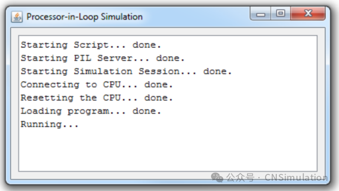
Figure 182, PIL running information window
During simulation, do not close this dialog box. Similar to the regular PSIM simulation method, you can display waveforms during or after the simulation.
2.4. Debugging PIL Simulation in TI CCS
When executing PIL simulation, you can debug the code in CCS. To debug the code, check the “Run Code Composer Studio in simulation” checkbox, as shown below.
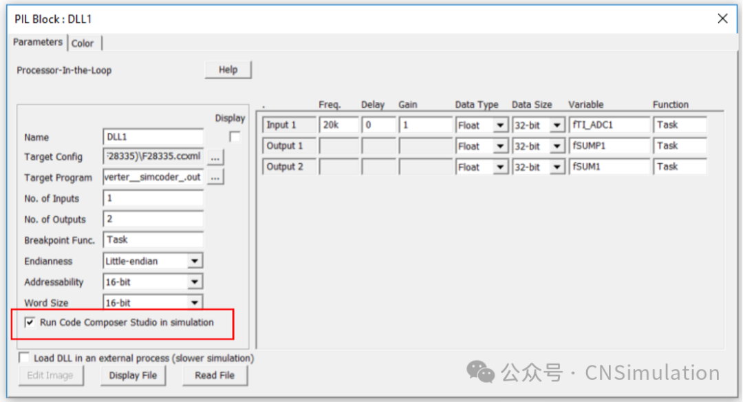
Figure 183, Checking to debug code in CCS
Click Run PSIM simulation to start the simulation, and the following dialog box will pop up:

Figure 184, Simulation startup prompt
CCS will start, and after it starts, click OK to close the pop-up window and begin PIL simulation. During the simulation, click the Pause Simulation icon in PSIM to pause the simulation; this icon is located to the left of the SIMVIEW icon in the toolbar, as shown below.
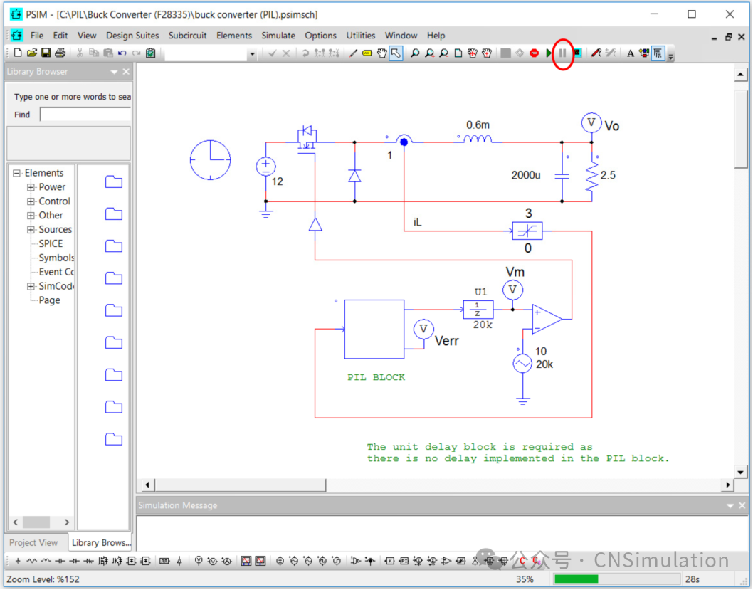
Figure 185, Simulation running in PSIM
Then return to CCS, and if you see the following information:
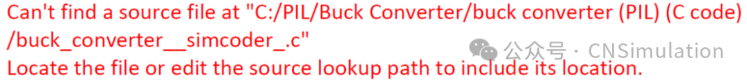
Click the Locate File… button, find the corresponding .c file in the folder, and after loading the .c file, the CCS window will display as follows:
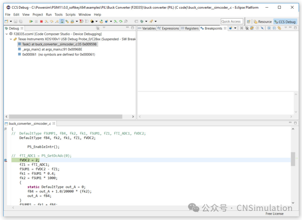
Figure 186, CCS display window information
You can set breakpoints for step-by-step execution, or use the previous methods to debug the code, checking the values of variables and registers.
After completing debugging in CCS, return to the PSIM interface and click Restart Simulation to resume the PIL simulation.
PIL simulation in PSIM is convenient to use and set up, providing an effective way to validate controller code in the absence of the power portion, while also allowing for various tests that are difficult to conduct on physical hardware, such as fault analysis, significantly speeding up the development process.