
Some Testing Service Projects:
-
Materials: Physical Properties, Chemical Analysis, Biological Tests
-
Reliability Testing of Components and Finished Products
-
Formula Analysis, Formula Restoration
-
Failure Analysis
-
Product Certification
National Customer Service Number: 4008180021
Add Customer Service WeChat anytesting001 to get daily R&D news
The following is the main text:
For those studying electronics, setting up test points on a circuit board is a very natural thing to do.
How many people have not heard of test points? How many know about test points but do not understand their purpose?
The basic purpose of setting test points is to test whether the components on the circuit board meet specifications and solderability. For example, if you want to check if a resistor on a circuit board has a problem, the simplest method is to use a multimeter to measure its ends.
However, in mass production factories, it is not feasible to slowly measure each resistor, capacitor, inductor, or even the IC circuits on every board with a multimeter, which led to the emergence of automated testing machines known as ICT (In-Circuit Test).
It uses multiple probes (commonly referred to as “Bed-Of-Nails” fixtures) to simultaneously contact all the components and circuits that need to be measured on the board, and then measures the characteristics of these electronic components in a sequential manner, primarily based on a sequence and secondarily in parallel.
Typically, testing all components on a standard board only takes about 1-2 minutes, depending on the number of components on the circuit board; the more components there are, the longer it takes.
However, if these probes directly contact the electronic components or their solder joints on the board, it could easily damage some electronic components, which would be counterproductive.
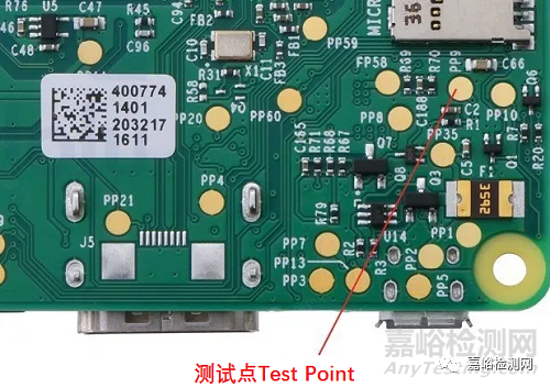
Therefore, clever engineers invented “test points,” which are a pair of small circular points extended from both ends of the components, with no solder mask on them, allowing the test probes to contact these small points without directly touching the measured electronic components.
In the early days when circuit boards still used traditional plug-in (DIP) components, the leads of the components were indeed used as test points because traditional component leads were strong enough to withstand the probe’s pressure, but there were often misjudgments due to poor probe contact.
Because general electronic components, after wave soldering or SMT tinning, usually form a thin film of solder paste flux residue on their solder surface, which has very high impedance, often causing poor probe contact.
So, it was common to see testing operators on the production line vigorously blowing air at the board with air guns or wiping the areas that needed testing with alcohol.
In fact, test points that have undergone wave soldering can also have poor probe contact issues. However, after SMT became popular, the instances of testing misjudgments were greatly improved, and the application of test points was significantly enhanced.
Because SMT components are usually very fragile and cannot withstand the direct contact pressure of test probes, using test points allows the probes to avoid direct contact with the components and their leads, which not only protects the components from damage but also greatly improves the reliability of testing, as the instances of misjudgment have decreased.
However, with the evolution of technology, circuit board sizes are getting smaller, and fitting so many electronic components onto such a small board is becoming quite challenging, leading to ongoing debates between design and manufacturing regarding the space occupied by test points.
Test points are usually circular because probes are also circular, making them easier to produce and allowing adjacent probes to be positioned closer together, thus increasing the density of the probe bed.
Using a probe bed for circuit testing has some inherent mechanical limitations, such as: the minimum diameter of the probes has a certain limit, and probes with too small diameters are prone to breakage and damage.
There are also certain limits on the distance between probes because each probe must come out of a separate hole, and the back end of each probe must also be soldered to a flat cable.
If the adjacent holes are too small, not only is there the risk of short circuits between probes, but interference from the flat cables is also a major issue.
Some high components cannot have probes installed beside them; if the probes are too close to high components, there is a risk of collision that could cause damage. Additionally, because these components are higher, holes must usually be opened on the testing fixture’s probe bed to avoid them, which indirectly results in an inability to install probes, making it increasingly difficult to accommodate all components’ test points on the circuit board.
As the boards get smaller, the number of test points is often discussed, and methods to reduce test points have emerged, such as Net test, Test Jet, Boundary Scan, JTAG, etc.
There are also other testing methods that aim to replace the original probe bed testing, such as AOI and X-Ray, but currently, each testing method seems unable to 100% replace ICT.
Regarding the probe planting capabilities of ICT, inquiries should be made to the cooperating fixture manufacturers about the minimum diameter of test points and the minimum distance between adjacent test points. Generally, there will be a hoped-for minimum value and a minimum value that can be achieved, but large-scale manufacturers often require that the minimum distance between test points not exceed a certain amount; otherwise, the fixtures may easily be damaged. (Source: Shared by members of Jiayu Testing Network)
Testing and Training Consultation Phone:4008180021
 R&D/Experimental Training Course Directory(Classes held year-round in major cities)
[Click Here] Electronics and Electrical Column